
 |
|
||||
BiographyBernhard Stampfer, born in 1989 in Austria, studied at the Technische Universität Wien where he received the Bachelor’s degree (BSc) in Electrical Engineering (2013), the Diplomingenieur degree (Dipl.-Ing., MSc equivalent) in Microelectronics and Photonics (2016) and the Doctoral degree (Dr.techn., PhD equivalent) in 2020. Bernhard is employed at the Institute for Microelectronics as a post-doctoral researcher and his work is focused on the characterization of defects in semiconductor devices. |
|||||
Defect Characterization using Deep Level Transient Spectroscopy (DLTS)
The performance of optical pn-junction devices such as photodiodes or solar panels can be negatively affected by electrically active defects in the semiconducting material, the dielectrics, or at the interfaces between them. These defects may be intrinsic to the starting material used for the device, but can also come from the processing steps performed to manufacture the device. Detailed knowledge about the type and characteristics of the defects contained is helpful in improving or tailoring the performance metrics of such devices, examples of which could include (depending on the type of device) its conversion efficiency, light sensitivity, or reaction speed. One method which provides this kind of capability is deep level transient spectroscopy (DLTS).
Deep level transient spectroscopy is a thermal scanning characterization method based on transient capacitance measurements as shown in Fig. 1. For pn-junction devices, the device under test (DUT) is first biased negatively to form a depletion zone. This negative bias is interrupted by pulses of higher bias, which causes defects to change their charge state. After returning to the low bias, these defects will revert to their previous charge states, thereby causing a change in the device capacitance which is measured during this phase. To increase the sensitivity of the measurement, many such cycles are recorded and averaged. This process is then repeated at a number of temperatures. As the characteristic charging and discharging times of the observed processes depend on temperature and the energetic alignment of the defects, an Arrhenius-like extraction as shown in Fig.2 can be used to calculate the energetic alignment and capture cross-sections of the contained defect species from the recorded decay times. Challenges for this characterizations method include the necessary measurement resolution of the transient capacitance measurements and the extraction of the characteristic decay times from the obtained data.
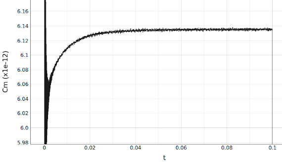
Fig. 1: Transient capacitance measurement after a positive bias pulse, showing the exponential recovery towards the equilibrium capacitance value. Note that this is a simple case with only a single defect species contributing to the measurement.
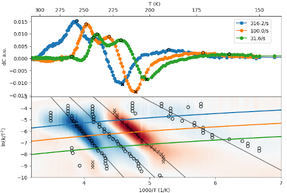
Fig. 2: Results from a DLTS measurement. Top: Capacitance change during specific time periods (rate windows) over temperature. Bottom: Arrhenius plot uncovering four defect species contained in the devices. Energetic alignment and capture cross-sections of the species are given by the slope and y-intersection of the fitted lines.