
 |
|
||||
BiographyViktor Sverdlov received his Master of Science and PhD degrees in physics from the State University of St.Petersburg, Russia, in 1985 and 1989, respectively. From 1989 to 1999 he worked as a staff research scientist at the V.A.Fock Institute of Physics, St.Petersburg State University. During this time, he visited ICTP (Italy, 1993), the University of Geneva (Switzerland, 1993-1994), the University of Oulu (Finland,1995), the Helsinki University of Technology (Finland, 1996, 1998), the Free University of Berlin (Germany, 1997), and NORDITA (Denmark, 1998). In 1999, he became a staff research scientist at the State University of New York at Stony Brook. He joined the Institute for Microelectronics, Technische Universität Wien, in 2004 and he is currently on a tenure-track position. His scientific interests include device simulations, computational physics, solid-state physics, and nanoelectronics. |
|||||
Topological Phase Transition in Transition Metal Dichalcogenide Nanoribbons
Employing novel 2D materials with topologically protected current-carrying edge states is promising for novel electronic devices. Interestingly, a monolayer-thin two-dimensional (2D) material can also exist in a 1T’ topological insulator (TI) phase. The fundamental band gap is opened by the spin-orbit interaction. The edge states are characterized by a linear dispersion which lies within the fundamental band gap. As there are no other electronic states within the band gap where the edge states may scatter, their conductive properties are enhanced. States could only backscatter.
These states localized at the edges are characterized by the spin-momentum locking. The two edge states with opposite spin polarization propagate in opposite directions along the same edge. Therefore, inducing a charge current along the edge results in the current with nonzero spin polarization. The spin-polarized currents are known to be the key to enable writing data in emerging magnetoresistive random access memories.
The edge states are protected against backscattering and carry the charge (and spin) current perfectly even at non-ideal edges typical to experiments. Performing a phase transition from the topologically non-trivial to a trivial insulating phase suppresses the existence of the edge states and the current flow. To do so, an electric field normal to the 2D sheet is applied. The bandgap in the inverted band structure is reduced, and can be completely closed upon increasing the electric field value. By further increasing the field, the bandgap reopens again; however, the traditional electron and hole band order is restored, indicating a topological phase transition from a non-trivial topological to a trivial insulator phase. In a nanoribbon, however, the gap between the sub-bands increases with the increase of the normal field, so that the sub-band spectrum remains gapped even at the critical electric at which the bandgap is closed in a 2D sheet. Even more, the sub-bands gap value increases for narrow nanoribbons. We found that the states are localized at the edges of a nanoribbon if their energies lie within the fundamental gap of a 2D TI. Fig.1 shows the imaginary parts of the wave vectors of the edge states’ wave functions. It decreases and becomes zero exactly at the electric field corresponding to the crossing of the edge mode dispersion and the bulk bands. As shown in Fig.2, the localization of the wave function qualitatively changes at this value of the electric field. One can define this point as a topological transition in a condoned geometry.

Fig. 1: Imaginary part of the wave vectors as a function of the normal electric field in a molybdenum disulfide nanoribbon of width 10 nm (stars), 20 nm (circles), and 30 nm (squares), for hole-like (left panel) and electron-like edge states (right panel).
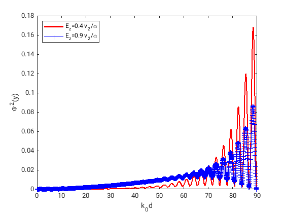
Fig. 2: The wave function of the electron-like edge states in a molybdenum disulfide nanoribbon of the width 50 nm. At low electric fields, the wave function is localized at the edge (red), while it moves towards the center of the nanoribbon at a higher field (blue).