
 |
|
||||
BiographyKonstantinos was born in Vayia, Greece, in 1994. He received the Diploma of Electrical and Computer Engineering from the University of Patras in 2018. Between 2018 and 2020, he studied at the Physics department of the National Technical University of Athens, where he received the Master's degree in Microsystems and Nanodevices. In February 2020, Konstantinos joined the Institute for Microelectronics, where he is currently working towards his doctoral degree, focusing on the characterization and modeling of charge trapping in low-noise silicon transistors. |
|||||
Evaluation of the Impact of Defects on Threshold Voltage Drift
The reliable function of MOSFET devices is seriously affected by oxide and interface defects that can change their charge state during operation by either charge capture or charge emission processes. These events affect the device's electrostatics and can lead to a drift in the device's characteristics. While the active number of defects per device in modern nanoscale devices is reduced, the impact of a single defect on the device characteristics dramatically increases. Consequently, charge emission events become visible as discrete steps in the device current, see Figure 1. Furthermore, it is observed that the increased contribution of the defects in scaled nodes leads to an increased variability between nominally identical devices, which makes them a severe challenge for robust electronic circuits.
Because of this, a statistical description is required to describe the overall contribution defects in nanoscale transistors. To do so, the complementary cumulative distribution function (CCDF) of step heights for each device kind needs to be created and analyzed (see Fig. 2). Uni-modal exponential distributions can explain the CCDFs for the following pMOS devices, that allow the extraction of the statistical parameters of the average impact of a single charge (η ) and the average number of defects per device (NT). To arrive at a detailed understanding of how device parameters can affect variability, we need to analyze data of devices with different gate areas. For this, we look at devices that exhibit the same gate area but different W and L. This allows us to verify the dependence of η and NT on the width and the length.
The complementary CDFs make it possible to study the geometry dependence of η and NT. The largest value for η and lowest NT is observed for the smallest available geometry. In contrast, the lowest η but largest NT is observed for the device with a large gate area. However, it can be observed that devices with the same area but different width/length ratios exhibit different values for η and NT. Furthermore, identical complementary CDFs can be observed for data extracted from devices with different gate areas. This leads to the conclusion that width and length must impact the statistically distributed parameters η and NT in a different manner. Thus the well-known relation η ∝1/(WL) is not fully accurate, at least not for the technology studied here.
As can be seen in Fig. 3, η is plotted against W√L. The extrapolation line shows that the scaling of W√L nicely captures all the data points experiments and DCM. This demonstrates that the scaling of statistical parameters can be better described with a W√L trend rather than the area of the devices WL typically used in literature.
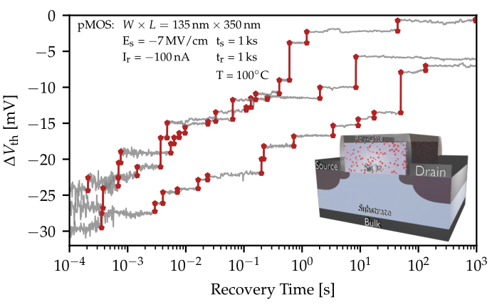
Fig. 1: Selected recovery traces showing the drift of the threshold voltage after NBTI stress, measured using scaled SiO2 pMOS transistors. The recovery proceeds in discrete steps. The emission events can be observed as positive discrete steps shown in red.
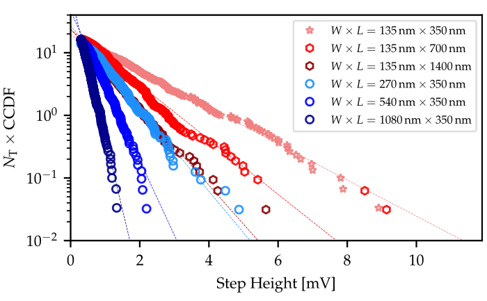
Fig. 2: {?}The CDF of step heights of extracted under the same measurement condition on pMOS devices with different geometries is shown. The data for extracted from devices with varying channel widths are shown in red, for varying channel lengths in blue.{?} A uni-modal exponential distribution can be used to describe the distribution (solid lines).
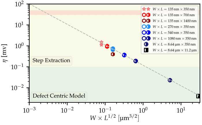
Fig. 3: The η values are plotted against W√L trend. The fitted line nicely captures both experimental values as well as DCM values. In some geometries, the markers for the experimental data and data from DCM model overlap as their values are really too close for a difference to be observed on the logarithmic scale used.