
 |
|
||||
BiographyMichael Waltl is an Assistant Professor of Robust Microelectronics, an IEEE Senior Member, and is the director of the device characterization laboratory at the Institute for Microelectronics. He obtained the BSc degree in electrical engineering, the degree of Diplomingenieur in microelectronics, and the doctoral degree in technical sciences (summa cum laude) from TU Wien in 2009, 2011, and 2016, respectively. His scientific focus is on reliability issues in semiconductor devices and circuits, where he is investigating bias temperature instabilities in silicon devices, devices employing wideband-gap materials, and transistors built on novel 2D materials. Dr. Waltl currently leads the Christian Doppler Laboratory for Single-Defect Spectroscopy and several FFG projects. Furthermore, Dr. Waltl heads several research projects with international industrial partners imec, ams AG, Lam Research, and more. In 2018 Dr. Waltl was a visiting researcher at imec, Belgium, Europe, and at Stanford University, CA, USA. His research group at the Institute for Microelectronics counts more than 10 scientists (PhDs and PostDocs). He is also the recipient of a best paper award at IRPS 2014, a best poster award at the ICPTDC 2019, and co-recipient of the best student paper awards at the IIRW 2019, IEDM 2019, and DRC 2020. Dr. Waltl serves in the management committee of the IIRW, is a member of the technical program committee of the ESREF and ESSDERC/ESSCIRC conferences, and is a reviewer of numerous renowned Journals including IEEE TED, Microelectronics Reliability, Journal of Applied Physics, and many more. |
|||||
Impact of Device Variability on the Performance of Electronic Circuits
Variations in the characteristics of transistors fabricated within the same process pose a remarkable challenge for the robust operation of electronic circuits — for instance, for the CMOS inverter circuit, see Figure 1. To ensure the stable operation of such circuits, simulations employing compact models describing the behavior of the transistors are typically performed during the design. For the simulations, SPICE tools are mainly used. However, the compact models employed often rely on mean values for the characteristic electrical parameters, e.g., threshold voltage, mobility, etc. In several simulation approaches, device-to-device variations are also considered. It has to be noted that transistor variability becomes increasingly important with nanoelectronics' scaling trend. Particularly for recent nodes where the device geometry is only a few tens of nanometers, the impact of defects located in the oxide or at the oxide/insulator interface becomes a critical issue. In more detail, the charge transitions of such defects appear as discrete steps in the current through the transistor (see Fig. 2). However, this has not been considered yet in circuit simulations.
A critical parameter in this context is the distribution of the step heights, i.e., the impact of the defects on the device characteristics. While most defects lead to a change in the device threshold voltage of a few millivolts, a certain number of traps can lead to a dramatic drift of the threshold voltage. Such "killer" defects can lead to the malfunction of electronics circuits and must be thoroughly considered during circuit design. In the case of the inverter circuit, a change in the device threshold voltage can change the signal propagation delay. To extract the signal propagation delay, SPICE simulations have been performed using Ngspice, considering a two-state defect model using trap parameters which have been calibrated from extensive measure-stress-measure experiments. For the simulations, an AC signal is applied at the input of the inverter, and the change in the threshold voltage of the transistors and the corresponding signal propagation delay is extracted. As shown in Fig. 3, while charge trapping at nMOS devices leads to a positive propagation delay, defects in pMOS transistors give rise to a negative propagation delay, and thus counteract the degradation introduced by the other device kind. As can also be seen, the majority of the propagation delay is caused by charge trapping in pMOS transistors. This is because the electron traps exhibit shorter trapping kinetics, and thus can follow the dynamics of the AC signal. The hole traps that reside in the pMOS exhibit, on average, larger emission times, and thus lead to a build-up of the propagation delay. It has further to be noted that, even at short total operational times of a circuit in the order of several tens of kiloseconds, the variation of the defect distributions among small-area devices of the same technology can introduce an additional signal propagation delay of several pico-seconds. Finally, it has to be noted that, while small variations may be negligible for AC signals in the 1MHz range, considering the influence of the single defects on the signal propagation delay can become particularly important for operating frequencies in the order of several hundreds of MHz or the GHz range.
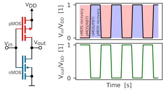
Fig. 1: The circuit diagram of the CMOS inverter is shown (left) together with the corresponding input and output bias signals (right). As indicated, one of the transistors is always under stress, while at the other, no gate-source voltage is applied. Note that the device stress can alter the characteristics of the devices, which might introduce additional propagation delays of the integrated circuits.
Fig. 2: In scaled transistors, the impact of defects on the device behavior can be observed as discrete steps in the current. Each step corresponds to a charge transition event of a defect. Consequently, device-to-device variability increases in scaled technologies, which has to be considered for the design of robust circuits.
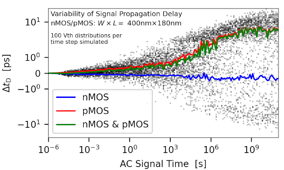
Fig. 3: The signal propagation delay of the CMOS inverter is shown over the AC signal time. For each transistor, different trap distributions have been calculated for AC operating conditions (black symbols). It can be seen that variations in the single-defect distributions cause a considerable distribution in the signal propagation delay.