
 |
|
||||
BiographyDominic Waldhör was born in Linz, Austria in 1992. He studied at the TU Wien, Vienna, Austria where he received the BSc degree in Electrical Engineering and the Diplomingenieur degree in Microelectronics and Photonics in 2018. He joined the Institute for Microelectronics in October 2018 where he works as PhD student. His current research focuses on the ab initio simulation of oxide defects in semiconductor devices. |
|||||
Local Stress Fields within Density-functional based Tight-binding
Mechanical stress plays a vital role in various processes important for the manufacturing of nanoelectronic devices. For example, strained silicon can be epitaxially grown on a silicon-germanium semiconductor alloy with a different lattice constant, which leads to increased electron mobilities in the strained-Si layer and enhanced overall device reliability.
Given current device dimensions reaching the few-nanometer regime, the common description of strain and stress within the framework of continuum mechanics breaks down. Hence, modeling those phenomena requires a treatment of mechanical stress at the atomistic level. While computational methods like Density Functional Theory (DFT) or Density-functional based Tight-binding (DFTB) are frequently used in material science to predict various electrical or optical properties in nanostructures, those approaches can only provide information on the global stress within the whole structure. However, a spatially resolved stress tensor field familiar from continuum mechanics is not available. In fact, it can be shown from first principles that such a field would be subject to certain gauge freedoms prohibiting a unique definition at the microscopic level.
We circumvent these fundamental limitations by exploiting the naturally arising decomposition of atomic forces into pairwise contributions within DFTB. By using these canonical pairwise forces, one can obtain a physically well-behaved stress tensor field following a well-known microscopic stress definition proposed by Hardy. We implemented this approach in the DFTB+ package by efficiently convoluting the pairwise stress virial with a smoothening Kernel in k-space.
We applied this method to study the local distributions of stress on a reconstructed Si(100) surface, as well as a defective carbon nanotube (CNT). As can be seen in Fig. 1, the Si surface itself is nearly stress-free due to the surface reconstruction, while most of the stress is concentrated in the transition layer from the surface to the bulk-like silicon-layer beneath. In a second example, we created a carbon divacancy in a CNT as depicted in Fig. 2. Clearly, the introduced defect induces positive and negative strain in its vicinity.
The stress fields obtained with our method provide a way to quantify and visualize microscopic stress in nanostructures, thus providing a computational tool to better understand strain-driven processes.
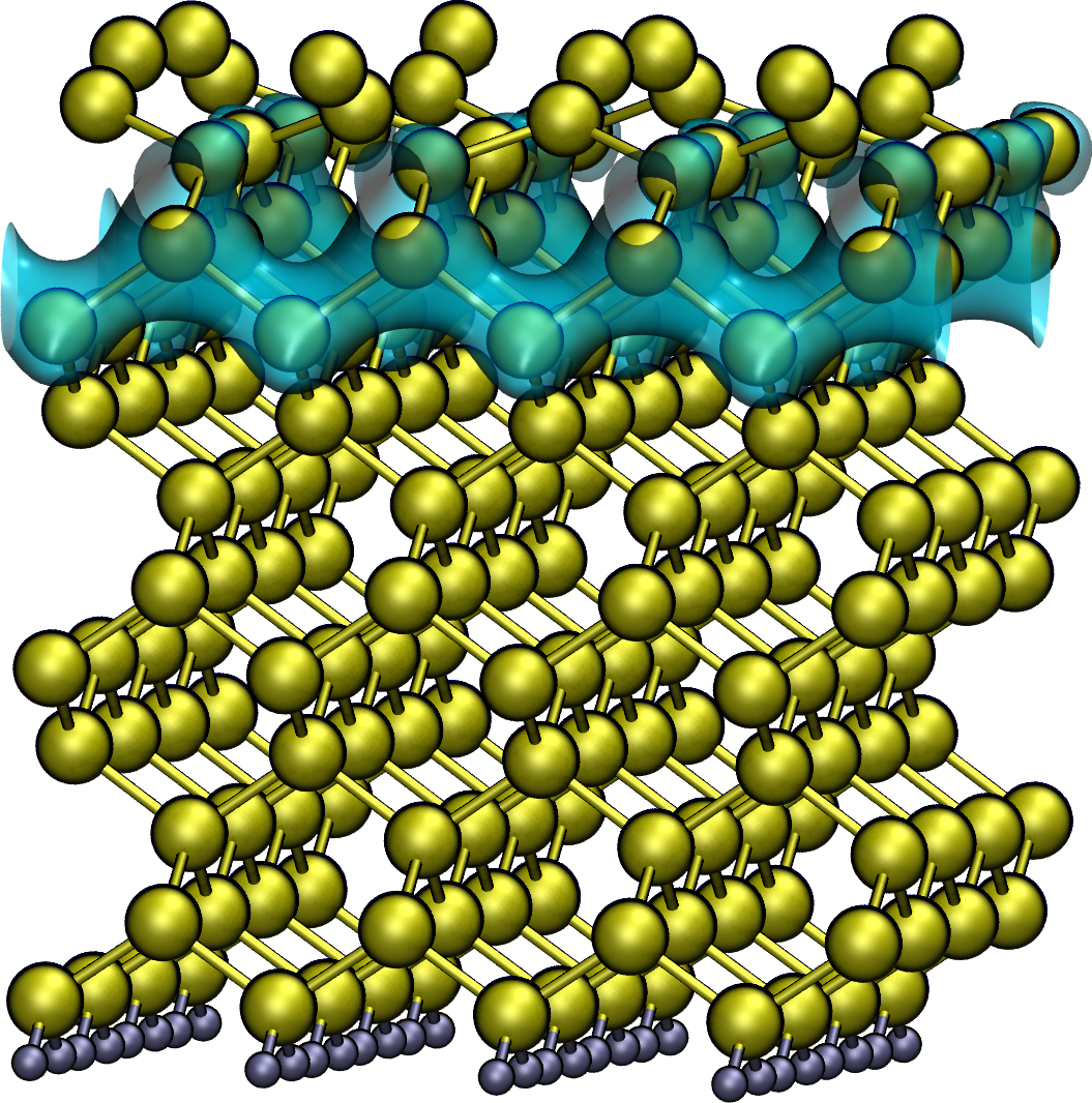
Fig. 1: Isosurface of the stress distribution underneath a reconstructed Si(100) surface.
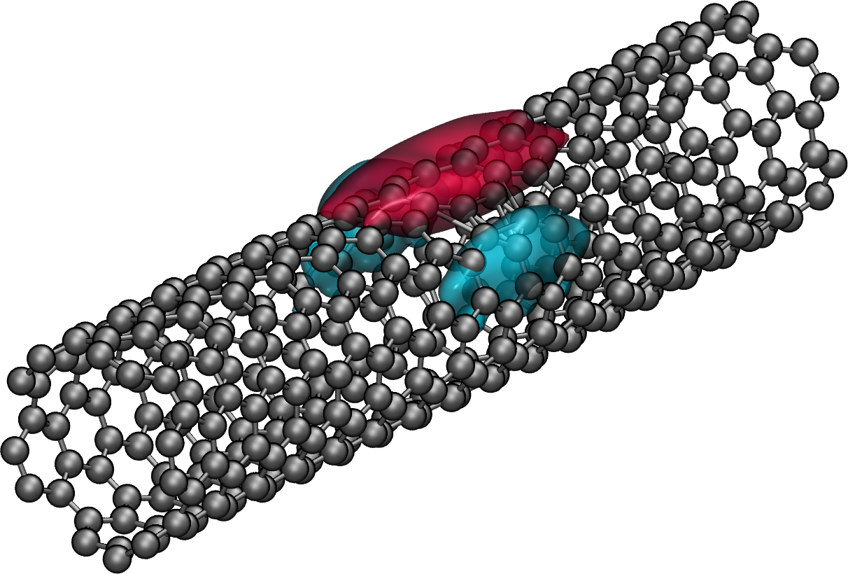
Fig. 2: Stress field induced by a carbon divacancy in a carbon nanotube. The stress is both compressive and tensile, as indicated by the different colors.