
 |
|
||||
BiographyTobias Reiter received his Bachelor's degree in Technical Physics in 2019 and is now enrolled in the Master Program Technical Physics, as well as the interfaculty Master Program Computational Science and Engineering, both at TU Wien, Austria. At the IµE he is employed in FFG project PASTE-DTCO, where his main focus is the developement and programming of the internally developed simulation framework ViennaLS. |
|||||
Modeling Plasma-Induced Damage During Dry Etching
Plasma processing is an indispensable tool for the fabrication of modern semiconductor devices. Especially in the design of modern three-dimensional (3D) devices, such as fin field-effect transistors (FinFET) or 3D NAND flash memories, high-energy plasma processes are essential to achieve fine patterning at ever-shrinking device scales. An accompanying issue with high-energy plasma exposure is plasma-induced physical damage (PPD) which is a side-effect of high-energy ion bombardment on silicon substrates or other material surfaces. This bombardment leads to a disruption of the crystalline nature of the underlying material and the potential introduction of defects, as shown in Fig. 1. Such damage can severely impact the device performance and reliability.
The semiconductor process simulator developed at the Institute for Microelectronics, ViennaPS, is used to study PPD during vertical channel hole etching in 3D NAND memory structures. The etching process in a Fluorocarbon plasma is modeled with an advanced surface kinetics model, utilizing a top-down Monte Carlo ray tracing approach to simulate particle fluxes of relevant species onto the surface. The plasma-induced damage is captured as a surface property, during the simulation of the etching process. A damage coefficient, which depends on the energy of the impinging ion, is defined, and assumed to decrease exponentially while etching the material surface. The final distribution of the surface damage then serves as input for a subsequent processing step, namely the selective epitaxial growth (SEG) of silicon at the bottom of the hole. Since SEG can only commence on a pristine, crystalline surface, the presence of a damaged layer leads to the formation of voids which severely impact the electronic properties of the device. Our developed model can accurately capture this behavior, as shown in Fig. 2.
We extend the model to a volume damage representation using a cell set to describe the silicon substrate underneath the surface. The ion damage inside the volume is captured with an adapted binary collision model using a Monte Carlo approach. The path of an ion is determined by launching a particle from the source plane above the surface and tracing its trajectory to find its direction and position upon impact with the surface. The ions are then assumed to travel through the material, experiencing a number of independent collisions with the silicon atoms. The energy transferred to the nuclei will cause damage to the silicon substrate, based on the Kinchin-Pease theory. Fig. 3 shows the results of the model, when applied to two different geometries: (1) a 7 nm-wide fin and (2) a vertical channel hole with a diameter of 40 nm. Due to the highly directional trajectories of the ions, the resulting damage is predominately confined to the bottom regions of the structures. However, we also observe some residual damage on the sidewalls, which is most likely caused either by reflected ions or by lateral straggling effects which is a consequence of ion scattering inside the substrate.
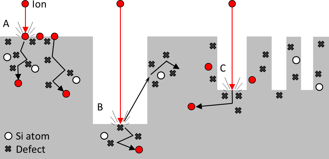
Fig. 1: Visual depiction of the physical plasma-induced damage mechanism in silicon-based devices during plasma processing, showing (A) typical physical damage, (B) sputtering, and (C) lateral straggling.
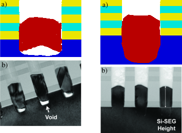
Fig. 2: (a) SEG at the bottom of the etched hole with the damaged layer present, showing the formation of voids. (b) The damaged layer has been removed in a low-energy post-etch treatment, and the SEG covers the entire bottom, leaving no voids. The simulation results are compared to experimental findings (C.-Y. Lung et al., ”Pre-epitaxial plasma etch treatment for the selective epitaxial growth of silicon in high aspect ratio 3D NAND memory”, in: 30th Annual SEMI Advanced Semiconductor Manufacturing Conference (ASMC), 2019).
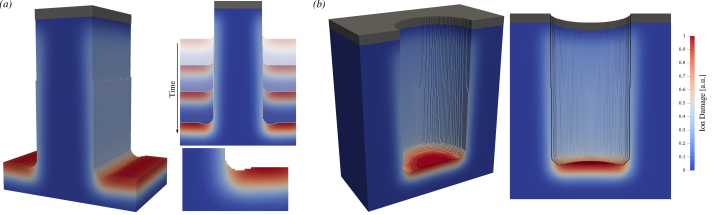
Fig. 3: The plasma etching simulation results for the (a) 7 nm fin and (b) 40 nm-diameter vertical channel hole. All simulations were conducted with an average ion energy of 100 eV. A 1 nm (a) or 8 nm (b) hard mask (gray) is placed on top of the structures, for which the PID is not recorded.