
 |
|
||||
BiographyMina Bahrami received her MSc. in condensed matter physics from the Amirkabir University of Technology of Tehran in 2021, where she studied a novel 2D material for the new generation of energy storage devices (i.e., lithium and sodium ion batteries). In June 2022 she joined the Institute for Microelectronics, focusing on ab-initio simulations of novel semiconductors and insulators in field-effect transistors. |
|||||
Evaluation of two Insulator Candidates for Nanoelectronics Based on 2D Materials
As electronic devices continue to scale below 5 nm, two-dimensional (2D) materials offer atomically thin channels that provide excellent electrostatic control and high theoretical mobility. However, their commercial integration is hindered by the lack of suitable gate insulators. This study investigates two promising candidates: strontium titanate (SrTiO3, STO) and bismuth oxyselenite (Bi2SeO5, BSO), the native oxide of Bi2O2Se, a high-mobility 2D semiconductor.
SrTiO3 has a cubic perovskite structure and exhibits a high dielectric constant (>300), making it highly effective for gate control. Bi2SeO5 also maintains a relatively high dielectric constant (~20) even in ultrathin layers and forms a structurally compatible interface with Bi2O2Se, creating a high-quality interface. DFT calculations using the PBE0 hybrid functional confirm that both materials exhibit favorable permittivities and band alignments, validating their potential for integration in 2D FETs.
Prototype devices were simulated and characterized: a back-gated MoS2/SrTiO3 FET and a top-gated Bi2O2Se/Bi2SeO5 FET. Both devices demonstrated good agreement between simulation and experiment. Hysteresis studies revealed clockwise (CW) behavior in BSO-based devices—attributed to electron trapping—and counter-clockwise (CCW) behavior in STO-based devices, likely due to mobile ionic defects or interfacial charge trapping.
Overall, both STO and BSO show strong potential as gate dielectrics in next-generation 2D FETs, with their performance governed by dielectric strength, band alignment, defect density, and interface quality. These findings offer valuable insights for designing scalable and reliable 2D electronic devices.
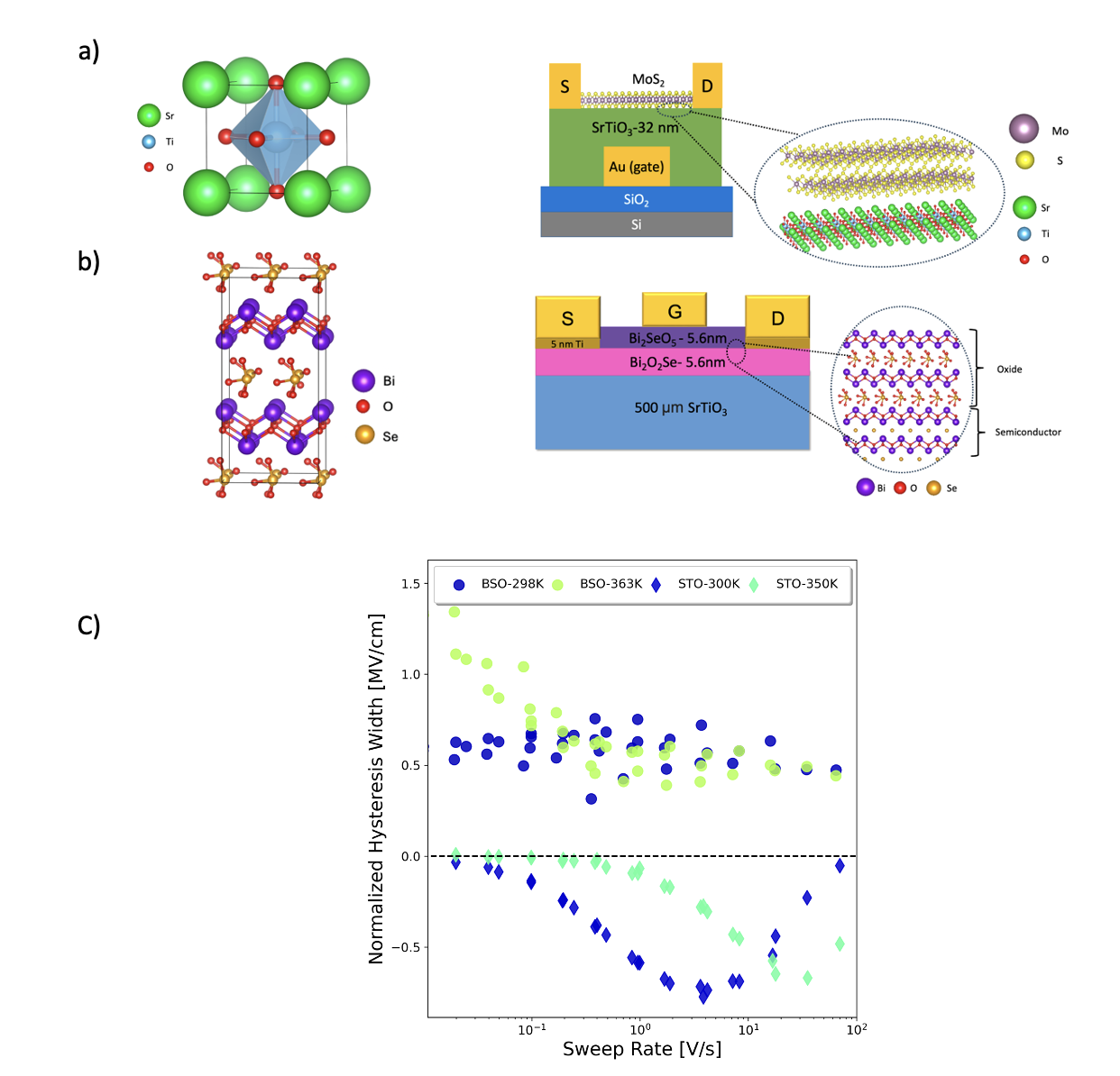
Fig. 1: a) Crystal structure of the cubic SrTiO3 perovskite, and schematic device geometry of the MoS2/SrTiO3. b) Crystal structure of the β-Bi2SeO5, and schematic device geometry of the Bi2O2Se/Bi2SeO5 devices. c) Hysteresis widths normalized by EOT at two temperatures for each device type