
 |
|
||||
BiographyBalázs Bámer was born in 1976, and received his MSc in 2001 at the Technical University of Budapest, where he studied computer science. After several years in industrial software development and various jobs in academia, he joined Institute for Microelectronics in January 2023 as a doctoral candidate in the Christian Doppler Laboratory for Multi-Scale Process Modeling of Semiconductors Devices and Sensors. His research focus is on studying dopant implantation and activation. In particular, he is working on a model for dopant activation in SiC, based on ion implantation conditions, such as temperature. |
|||||
Cluster-based semi-physical model for dopant activation
Technology Computer-Aided Design (TCAD) software suites are essential in simulating and designing semiconductor manufacturing processes. They can substitute time-consuming and expensive experiments by accurately simulating the various processing steps, such as ion implantation, annealing, etching, oxidation, etc.
Today, mainly ion implantation is used to dope semiconductors. Its main drawback is its induced damage to the semiconductor crystal structure. Subsequent processing steps, like annealing, can be used to repair the crystal structure and activate the dopant atoms.
Our aim is to develop a simulation model capable of predicting the added annealing effect of different processing steps. The current empirical models are unable to simulate these added effects since they only consider the implantation conditions, such as the implant dose and temperature.
We are building a semi-physical model to describe the behaviour of the various species in the semiconductor. These are the dopants on lattice points, point defects, dopant-defect pairs, and clusters of different sizes. We define the possible reactions between them, including the reaction kinetics and use a set of ordinary differential equations (ODEs) to model the time evolution of the concentration of the different species during annealing.
We investigate two ways to elucidate the post-implant conditions of the semiconductor film. Some of these concentrations are not measurable and can only be calculated through time-intensive atomistic simulations, which we will apply to verify and calibrate our model.
First, we used a global optimiser to assess the spline control nodes describing the initial concentrations of the species. This enabled us to obtain the initial concentrations as a function of doping concentrations, at a specific annealing temperature.
Second, to get the initial concentrations as a function of both doping concentrations and annealing temperature, we use a physics-informed neural network (PINN), where the neural network itself gave the set of approximating functions.
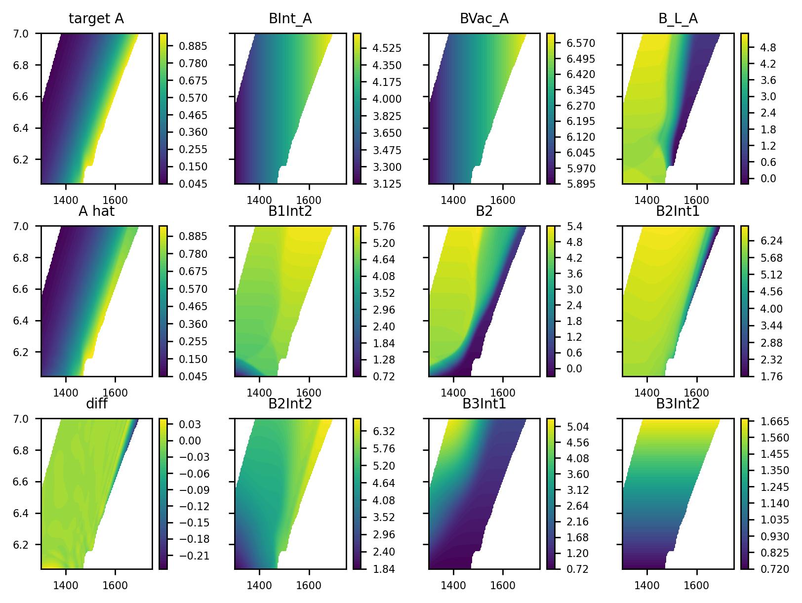
Fig. 1: Initial concentrations of the simulated species as a function of annealing temperature and doping concentration using PINN. All the concentration values are shown as base-10 logarithm of values in 1/μm3