
 |
|
||||
BiographyMohammad Davoudi received his bachelor's in Atomic and Molecular Physics from the Iran University of Science and Technology. He then started his master's in Particle Physics at Shahid Beheshti University where his research focused on Entanglement Entropy, Quantum Chromodynamics, and Gauge/Gravity duality (AdS/CFT). After graduation in 2019, he taught physics as a lecturer at the University of Eyvanakey. In June 2022 he joined the Institute for Microelectronics, working on novel semiconductors and insulators for the next generation of electronic devices, specifically FET transistors. |
|||||
Multi-Scale Modeling of Bi2O2Se/Bi2SeO5 FETs
As electronic devices continue to scale toward nanometer dimensions, two-dimensional (2D) materials have emerged as promising candidates for next-generation field-effect transistors (FETs). Their atomically thin structure offers excellent electrostatic control and reduced short-channel effects, making them ideal for sub-5 nm technologies. However, realizing high-performance and reliable 2D devices hinges on identifying suitable combinations of semiconductors and gate dielectrics. The integration of a 2D semiconductor with a high-κ dielectric that forms a clean, stable interface remains a significant challenge. We investigate a novel material system based on the high-mobility 2D semiconductor (Bi2O2Se) and its native oxide (Bi2SeO5) as the gate insulator. This pair offers several advantages, including chemical stability, favorable band alignment, and a layered structure that naturally forms a van der Waals heterostructure with minimal interfacial defects. Using a multi-scale modeling framework, we combine density functional theory (DFT) to extract key material parameters with TCAD simulations calibrated against experimental data to model device behavior.
Our approach includes comprehensive simulation of electrostatics, charge transport, and reliability-related effects such as hysteresis and threshold voltage instability. We incorporate parameters such as mobility, interface trap densities, and Schottky barrier heights into the TCAD model. Simulations show excellent agreement with experimental transfer and output characteristics across varying temperatures and biases. We further analyze hysteresis behavior using a non-radiative multiphonon (NMP) trapping model and extract trap parameter distributions using an Effective Single Defect Decomposition (ESiD) method.
This integrated modeling approach not only explains the experimentally observed behavior of Bi2O2Se/Bi2SeO5 FETs but also provides a robust methodology for evaluating new 2D semiconductor/insulator systems. These insights are essential for guiding the design of scalable and reliable 2D nanoelectronic devices.
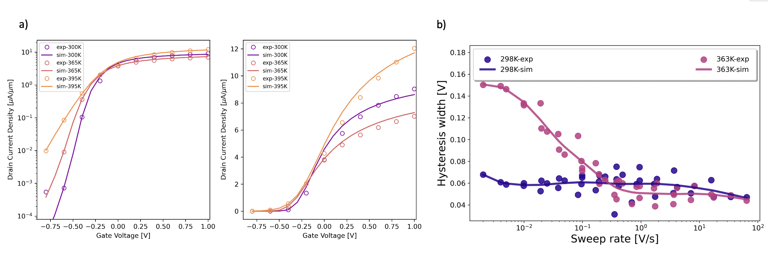
Fig. 1: a) Transfer characteristics for a Bi2O2Se/Bi2SeO5 device at 300 K, 365 K, and 395 K. b) Comparison between the simulated and measured hysteresis widths. The solid lines and circles represent simulation results and experimental data respectively