
 |
|
||||
BiographyPedram Khakbaz was born in Arak, Iran. He received his Ph.D. degree in electronics engineering from the University of Udine, Italy, in 2022 where he studied the electronic transport in devices based on two-dimensional semiconductors. From Sep. 2016 to Sep. 2018, he was with the computational nano-electronics lab and finished his M.Sc. degree in nano and micro-electronics engineering at the University of Tehran, Iran. In June 2022, Pedram joined the Institute for Microelectronics as a postdoctoral researcher and his current research interests include ab initio modeling and quantum transport for the modelling of devices based on 2D semiconductor materials. |
|||||
Intrinsic Properties of the 2D Bi2SeO2 and Its Native Insulators
Achieving atomic-level control over both the channel and gate insulator is critical for scaling field-effect transistors beyond the sub-nanometer node. A notable breakthrough in this direction involves the systematic layer-by-layer oxidation of the two-dimensional semiconductor Bi2SeO2, which leads to the formation of an atomically thin gate dielectric, bismuth oxyselenite (Bi2SeO5). This oxidation process yields a single-crystalline, atomically flat, and nearly lattice-matched interface between the semiconductor and its native oxide. The resulting β-phase of Bi2SeO5 incorporates SeO3 tetrahedra between intact Bi2O2 layers, maintaining structural integrity with the parent material.
To evaluate its suitability for device integration, the electronic and dielectric properties of Bi2SeO2 and its native oxides were examined. The Bi2SeO2/Bi2SeO5 system fulfills the preferred combination of a low effective mass semiconductor and a higher mass insulator. The high out-of-plane dielectric constant of the oxide allows thicker layers without sacrificing electrostatic control, while the large dielectric constant of the channel material supports enhanced mobility by effectively screening charged defects and phonons. However, high in-plane permittivity in both materials may increase drain-induced short-channel effects, necessitating careful architectural choices such as FinFET or gate-all-around designs. The thermal stability of β-Bi2SeO5 was evaluated using molecular dynamics simulations up to 450 K. The SeO3 tetrahedra exhibited rotational dynamics yet preserved their coordination throughout, and all simulated structures relaxed back to the original geometry after optimization, as illustrated below.
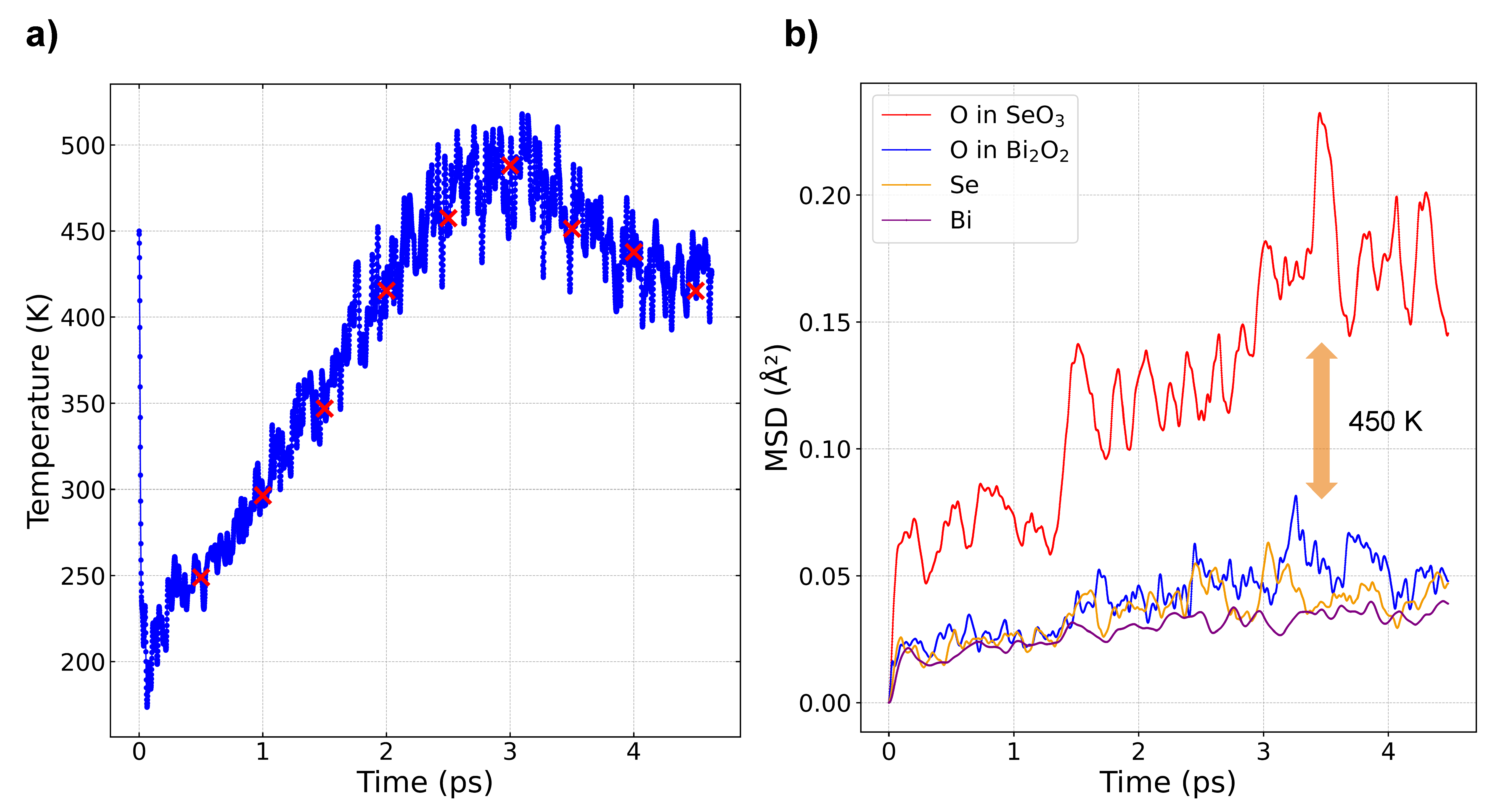
Fig. 1: (a) Temperature evolution during molecular dynamics simulations of β-Bi2SeO5 up to 450 K, with red crosses marking extracted snapshots used for geometry optimization. All configurations converged back to the original structure. (b) The mean square displacement highlights that the O atoms in the SeO3 units, displaced considerably more than the other atoms.