
 |
|
||||
BiographyDavid Lamprecht was born in South Tyrol, Italy, and received both his Bachelor and Master’s degrees in Physics at the University of Vienna in the Physics of Nanostructured Materials (pnm) Group of Prof. Jani Kotakoski. David joined the Institute for Microelectronics in June of 2023, where he is pursuing a PhD degree with a focus on understanding the impact of the adsorption of ambient gas molecules on the surfaces of 2D semiconducting films and on the performance of devices and sensors based on these. He works in close cooperation with his former group and uses the Nion Ultra-STEM 100 scanning-transmission electron microscope located at Sternwarte Park, Vienna to characterize 2D materials like Mos2. |
|||||
Two-step substitutional doping of MoS2 observed by combined HAADF and SSB imaging
Substitutional doping with heteroatoms has been shown to significantly enhance the catalytic activity and gas sensitivity of MoS2. While the heteroatom replacement of Mo and S atoms has been explored for various elements, many studies lack unambiguous atomic-scale evidence, mostly due to surface recontamination between modification and imaging steps. Due to the unique layout of the ultra-high vacuum (UHV) system at the Sternwarte lab of the Kotakoski group (Uni Wien), we are able to introduce Mo and S defects in monolayer-MoS2 via helium plasma irradiation, repopulate the defective sites with heteroatoms via evaporation and subsequently analyze the resulting structures with scanning-transmission-electron microscopy (STEM) without exposition to ambient conditions.
For structural analysis, we employ high-angle annular dark field (HAADF) imaging and single-side-band (SSB) phase reconstruction ptychography. HAADF imaging offers insights into the elemental composition of the samples, but is limited by the beam-sensitivity of defective MoS2. In contrast, aberration-corrected SSB reconstruction of 4D-STEM data gathered by a direct electron detector allows simultaneous imaging of high and low Z elements at significantly lower doses. By combining these techniques we gain insight into the produced defect structures as well as into the local structure of Pt atoms substituting Mo and S atoms.
In a recent study we show that with SSB we can reliably distinguish between Pt atoms trapped in S mono- or divacancies, Mo vacancies and adatoms, see Fig. 1. Our combined implantation and analysis methods open the way for systematically introducing controlled dopants into MoS2. By tuning the ion beam parameters and incorporating a resulfurization step to heal remaining sulfur vacancies, this may in the future be adapted for larger-scale applications allowing for precise control over dopant placement.
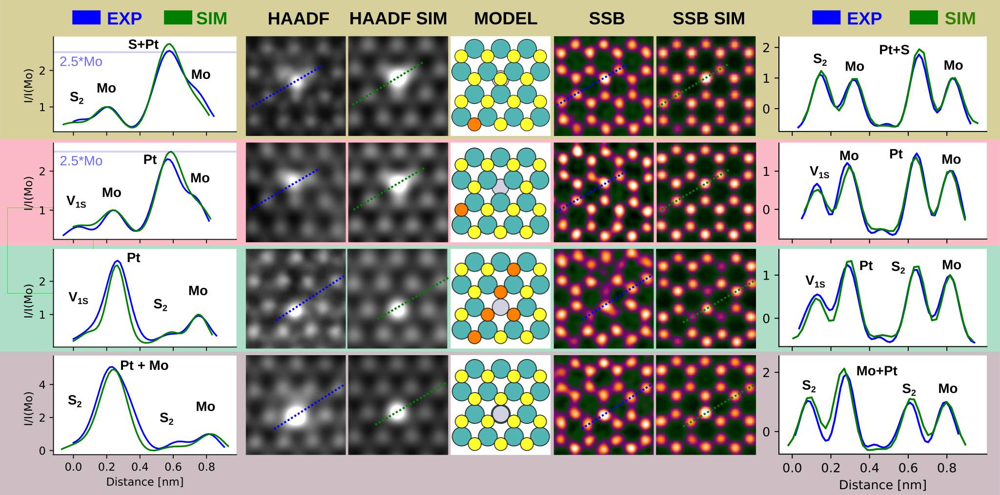
Fig. 1: From top to bottom: HAADF images, SSB images, abTEM simulations and the corresponding line profiles of Pt atoms in single S, double S and Mo vacancies, as well as Pt adatoms.