
 |
|
||||
BiographyAlexandros was born in Athens, Greece, in 1997. In 2020, he completed his undergraduate studies in Physics at the University of Crete and continued his graduate studies there in collaboration with the FORTH Institute where he obtained his diploma in 2022. His previous research activities were on RF MEMS with Silicon Nitride and on High Frequency diodes based on Carbon Nanotubes and fullerene derivatives. In 2022, he joined TU Wien to pursue his PhD and his current research is on electrical characterization and device fabrication of 2D material based FETs. |
|||||
Ivestigation of Random Telegraph Noise on 2D FETs
Random Telegraph Noise (RTN) is a phenomenon observed in electronic devices where the current fluctuates between discrete levels over time due to charge trapping and detrapping events. In nanoscale field-effect transistors (FETs), these fluctuations become more pronounced due to reduced screening and the high surface-to-volume ratio. RTN is particularly important to study in 2D FETs because it directly impacts device stability and reliability, which are critical factors for their integration into next-generation low-power and high-performance electronics.
RTN originates from charge carriers being intermittently captured and emitted by trap states located near the conduction channel—typically at the dielectric/semiconductor interface or within the oxide. These events cause the drain current to jump between high and low states, as illustrated on the right figure. The average time a trap spends in the empty or occupied state is referred to as the emission time (τe) or capture time (τc), respectively. While this phenomenon is also present in traditional 3D silicon-based FETs, it is more severe in 2D FETs due to their atomic thickness and increased sensitivity to interface quality. As shown in the left part of the figure, RTN can be visible even during standard ID–VG measurements, at different frequencies
To thoroughly investigate RTN in 2D FETs, time-domain measurements are conducted at fixed bias conditions where current traces are monitored over time. These measurements aim to accurately resolve the discrete RTN steps and quantify τc and τe. By analyzing their temperature dependence, one can extract key parameters such as the activation energy. This characterization sheds light on the nature and location of the traps but also aids in optimizing dielectric interfaces and fabrication processes to mitigate RTN, something essential for the advancement of reliable 2D electronic devices.
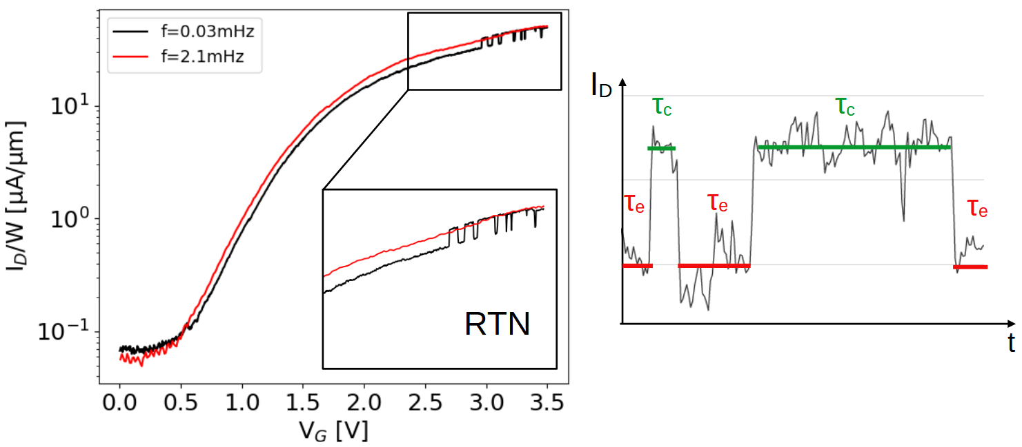
Fig. 1: An ID-VG showing a sweep frequency dependent trap (left) and an RTN signal at a constant VG (right).