
 |
|
||||
BiographyAlexander Simko was born in Ystad, Sweden, in 1999. He began studying electrical engineering at Lund University in 2019, and after an exchange semester at ETH Zürich in 2023, he completed his master’s degree in June 2024. During his master’s thesis, he worked on TCAD simulations of vertical GaN FinFETs. Alexander joined the Institute for Microelectronics in July 2024, where his research focuses on TCAD simulations of SiC devices. |
|||||
Simulating Scaling Effects in Fully Vertical GaN FinFETs
Vertical GaN FinFETs for power applications is a novel device concept with several advantageous properties. They do not require a p-type layer, making it unipolar which improves switching losses as there are no reverse recovery charges. The double gate design around the fin improves electrostatic control allowing for normally-off behavior. One drawback of a FinFET design is the lower interface mobility compared to a AlGaN/GaN heterostructure device. Devices with breakdown voltages above 1200 V, low on state resistance and subthreshold swings close to the ideal limit as well as high operating current densities have been demonstrated, however there are many dimensions that can be optimized in order to improve performance.
To help investigate possible design options TCAD simulations were used to explore the parameter space. In order to ensure accurate results the models needed to be calibrated. In particular, as the MOS-interface mobility plays a central role, it had to be modeled well. At higher gate voltages the effective mobility decreases, as the charges are pushed closer to the interface.
With the calibrated models, a large number of simulations could be run to explore possible designs. The results show that FinFETs with a long drift layer can reach values close to the GaN material limit, if scaled properly, as can be seen in the figure below.
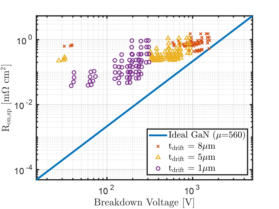
Fig. 1: Simulated specific on state resistance versus breakdown voltage compared to ideal GaN behaviour.