
 |
|
||||
BiographyAxel Verdianu received his master’s degree in Microelectronics and Photonics from the Vienna University of Technology in 2024. During his studies he spent one semester abroad at the KU Leuven, Belgium. For his master’s thesis he focused on reconfigurable field-effect transistors (RFET) at the Institute of Solid State Electronics. In February 2024 he joined the Institute of Microelectronics and is now pursuing his PhD studies where his research is focused on the fabrication and electrical characterization of 2D material-based field-effect transistors. |
|||||
Comparing hysteresis measurement results across different device technologies
Hysteresis measurements, which quantify the trap charge difference between the up and down gate voltage sweeps, serve as a crucial reliability metric for evaluating 2D electronic devices. However, comparing hysteresis across different device technologies is challenging due to variations in measurement conditions and material properties. As illustrated in Figure 1, the observed hysteresis measured on the very same device strongly depends on the selected gate voltage range. This dependency arises because different gate voltages shift the Fermi level, thereby altering the charge carrier density within the device and impacting the interaction with trap states. Furthermore, the location of the trap band inside the gate oxide and its energetic alignment with the underlying semiconductor play a significant role. The relative positioning determines which traps are activated or filled under specific biasing conditions. As a result, the applied gate voltage during hysteresis measurements can significantly affect the outcome, making it difficult to isolate the intrinsic properties of the device from measurement-induced artifacts. To enable meaningful comparison between different device technologies, a consistent and reproducible method for defining the gate voltage range is essential. This method must ensure that the Fermi level is scanned across the same energy window in all devices, regardless of their individual band structures or threshold voltages. A standardized approach will provide a more accurate and reproducible reliability assessment in 2D devices and facilitate benchmarking across diverse material systems and device architectures.
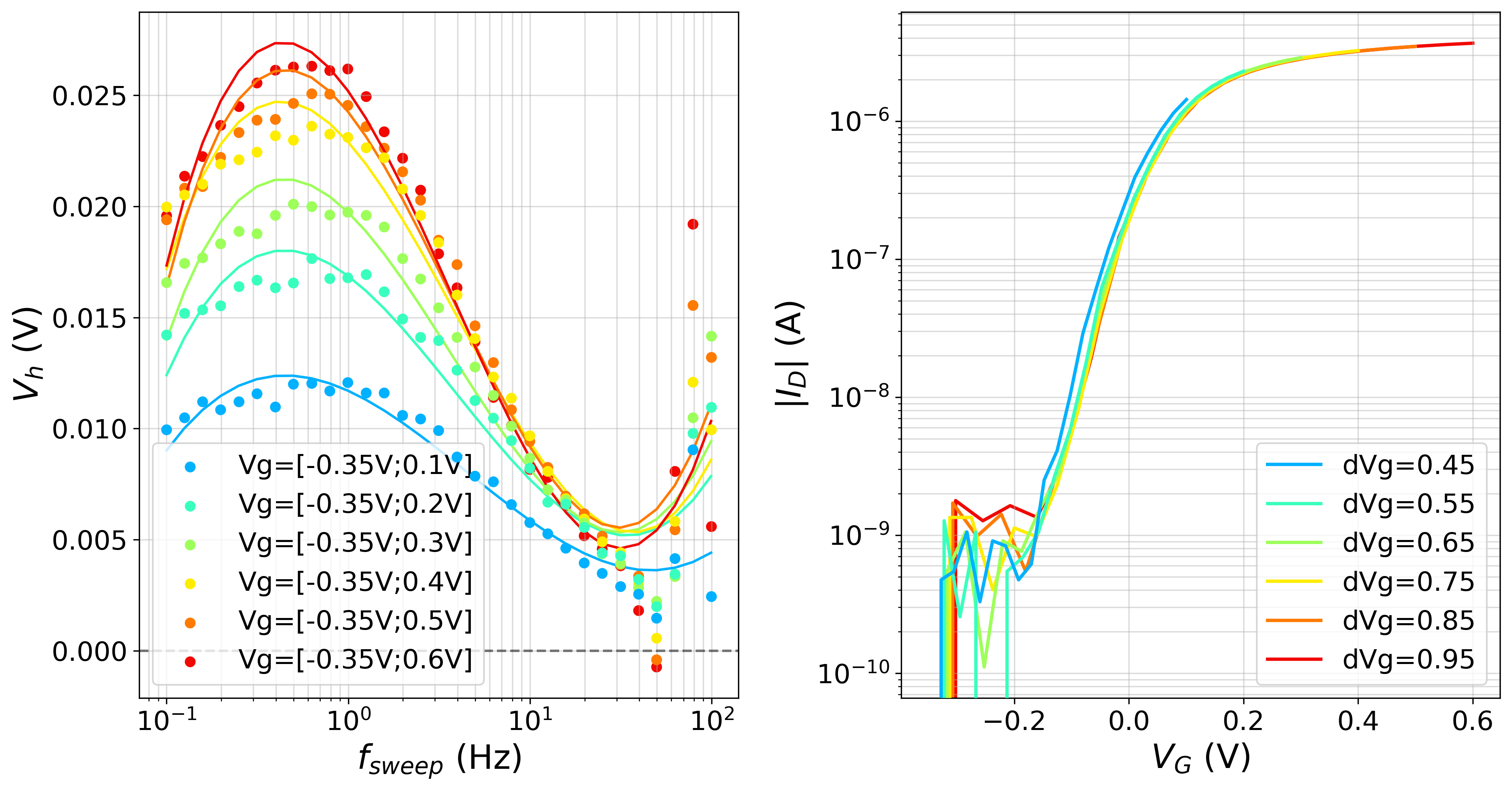
Fig. 1: The left plot in Fig. 1 shows the hysteresis increase with higher maximum gate-voltages, while the minimum gate voltage was kept constant. Note that the hysteresis magnitude is increasing with increasing gate voltages while the hysteresis peak frequency and overall shape remain unchanged. Fig. 1, right, illustrates the transfer curves of the corresponding gate voltage ranges and gives the total gate voltage range (dVg).