 |
|
||||
BiographyTheresia Knobloch is a postdoctoral researcher focusing on fabrication, experimental characterization, and physical modeling of nanoelectronic devices based on 2D materials. She obtained her doctoral degree from TU Wien in 2021 and performed parts of her Ph.D. research as a visiting scholar at Purdue University, USA in 2018 and 2019 and Soochow University, China in 2017. For her work, she received several awards including the IEEE EDS Ph.D. Student Fellowship in 2021 and the Best Student Paper Award at the DRC in 2020. She joined the Institue for Microelectronics in 2016 while completing her master's degree in microelectronics and photonics. She acquired both her M.Sc. in 2016 and her B.Sc. in technical physics in 2014 from TU Wien with distinction. Currently, she primarily studies the electrical stability and reliability of 2D material-based field-effect transistors. |
|||||
Gate Leakage Currents in Ultra-Scaled 2D Transistors
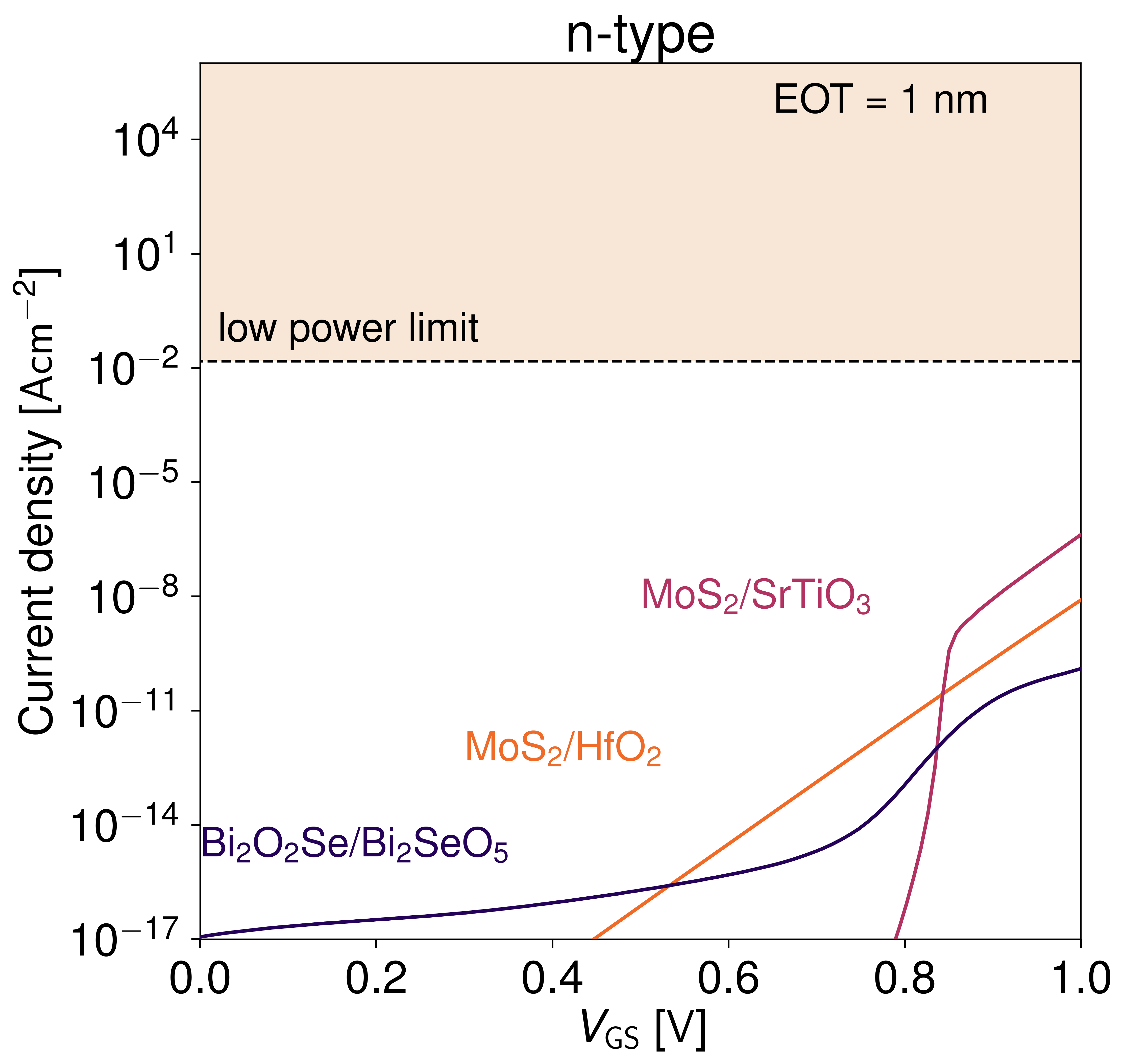
Scaling transistors down to below 5nm channel lengths requires reducing the channel thickness to mitigate short-channel effects. In this context, layered 2D semiconductors show promise as they can provide excellent electrostatic control. Critical performance aspects of 2D FETs are defined by the gate insulators. Importantly, the gate insulator must offer sufficient capacitive control while effectively blocking leakage currents. Two promising candidates for such scaled gate insulators are strontium titanate (SrTiO3, STO) and the native oxide of bismuth oxyselenide (Bi2SeO5, BSO). STO, which crystallizes in a cubic perovskite structure, exhibits a bulk permittivity exceeding 300 at room temperature. Meanwhile, BSO has a dielectric constant of about 20 and forms a high-quality zipper interface with Bi2O2Se, making it well-suited as a gate dielectric in ultra-scaled devices. To quantify gate leakage currents in representative metal-insulator-semiconductor (MIS) stacks using gold (Au) as a top gate, we investigate Au/STO/MoS2 and Au/BSO/Bi2O2Se gate stacks. Tunneling currents through these gate stacks, each with an equivalent oxide thickness (EOT) of 1nm, are modeled using the Tsu-Esaki approach within the Comphy framework. The most important model parameters are the insulator thickness, energy barrier heights, and effective tunnel masses. Figure 1 compares the resulting leakage currents for an applied gate bias of up to 1V, revealing that both MoS2/STO and Bi2O2Se/BSO stacks maintain leakage currents several orders of magnitude below the 10−2 Acm−2 low-power limit. In conclusion, SrTiO3 and Bi2SeO5 both effectively limit gate leakage currents in ultra-scaled 2D transistors. Their high-κ properties and favorable interface qualities make them excellent candidates for next-generation nanoelectronic applications.

Fig. 1: Calculated gate leakage currents.


