
 |
|
||||
BiographyChristoph Wilhelmer was born 1993 in Lienz, Austria. He received his Bachelor degree in Technical Physics from TU Wien after doing an exchange semester at the University of Bath, UK in 2017. He received his Diplom-Ingenieur degree in Technical Physics from TU Wien in 2020 where he carried out his Master Thesis in the Quantum Materials group of the Institute of Solid State Physics. In March 2020 he joined the Institute for Microelectronics where he started his PhD, focusing on defect creation mechanisms in oxides used for semiconductor applications. |
|||||
First-principles investigations of noise in monolayer WSe2 field effect transistors
The implementation of 2D semiconductors in field effect transistors (FET) is a promising approach to decrease the spatial dimensions of the device. However, such 2D FETs still lack the reliability to be produced on an industrial scale. This limitation arises from the high defect densities present in 2D materials, which degrade the performance of electronic devices. In particular, specific defects can lead to random telegraph noise (RTN) in FETs due to capture and emission of charge carriers.
Measurements and subsequent TCAD simulations suggest that the RTN traces in the ultra-scaled devices originate from hole trapping at fast defects in the 2D substrate [1]. Additionally, the microscopic origin of the RTN signals was investigated with density functional theory in conjunction with a hybrid functional. Based on STEM imaging, the types of defects occurring in the monolayer WSe2 film were identified. The relaxed defect structures calculated in the positive and neutral charge state are shown in Fig. 1. The charge transitions at the hole-trapping defect types Se vacancy (VW) and Se antisite (SeW) in monolayer WSe2 were then characterized according to a non-radiative multi-phonon model [2].
The hole charge transition levels (CTLs) of both defect types are close to the valence band edge of WSe2 with relaxation energies for charge capture and emission below 0.2eV. In combination with the TCAD simulations [1], it is demonstrated that both investigated defect types exhibit defect parameters within the energy range to explain the detected RTN signals.
[1] H. Ravichandran et al., Nat. Commun. 15,10562 (2024). doi:10.1038/s41467-024-54283-1
[2] A. Alkauskas et al., Phys. Rev. B90, 075202 (2014). doi:10.1103/PhysRevB.90.075202
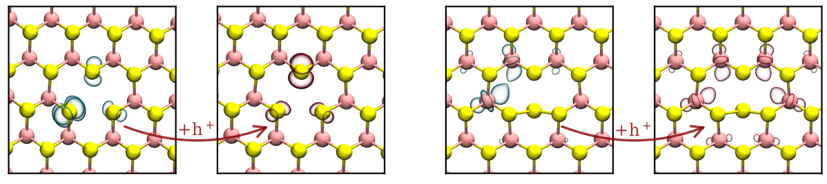
Fig. 1: Left: VW in neutral and positive charge state after trapping a hole h+ and subsequent structural relaxations. Right: SeW in neutral and positive charge state after trapping a hole h+ and subsequent structural relaxations. The highest occupied (blue) and lowest unoccupied (red) molecular orbitals are drawn at an isovalue of 0.05 e/Å3.