
 |
|
||||
BiographyKonstantinos was born in Vayia, Greece, in 1994. He received the Diploma of Electrical and Computer Engineering from the University of Patras in 2018. Between 2018 and 2020, he studied at the Physics department of the National Technical University of Athens, where he received the Master's degree in Microsystems and Nanodevices. In February 2020, Konstantinos joined the Institute for Microelectronics, where he worked towards his doctoral degree, focusing on the characterization and modeling of charge trapping in low-noise silicon transistors. He defended his Disertation in the scope of the CDL for SDS project on Feb 28th, 2024 |
|||||
Evaluation of the Impact of Body Bias on the Threshold Voltage Drift of SiO2 Transistors
As complementary metal-oxide semiconductor (CMOS) devices have continued to shrink in size over the past few decades, the number of defects affecting nanoscale device performance has significantly decreased. Likewise, there has been a reduction in the number of substrate dopants responsible for the percolative way of conduction in the inversion layer, which is typically assumed for scaled nodes. However, the impact of defects on the device electrostatics increases with scaling due to the enhanced repulsion of a charged defect in weaker inversion layers. Notably, there is a rise in both the time-zero and time-dependent variability, signifying a decrease in device reliability. Due to this, a statistical approach is required to evaluate charge-trapping effects at the single-defect level, which can lead to increased variance on device parameters such as Vth. In this context, the body bias (BB) can play a pivotal role in the effect of individual charged defects on the device behavior. Thus, the impact of individual charged gate oxide defects on nanoscaled MOSFETs needs to be investigated as a function of the bias voltage VB. To describe the contribution of single defects to the threshold voltage drift ΔVth, we create the statistical distributions of the step heights observed from the emission events during stress-recovery measurements. The complementary cumulative distribution functions (CCDF), seen in Figure 1, describe the collected step heights for pMOS devices of the same geometry under different bias conditions. Exponential distribution functions, marked with dashed lines, are utilized to describe the experimental distributions, enabling the extraction of the average impact of defects on the ΔVth (η).
The extracted η values, normalized to the gate area, can be seen in Figure 2 against VB values. All geometries depend similarly on VB. The increase of VB towards reverse body bias (RBB) conditions leads to increased η values, while forward body bias (FBB) leads to decreased ones. To examine this behavior further, TDDS measurements are performed for two different BB conditions on a device with a dominant oxide trap, as depicted in Figure 3. The BB seemed to impact the step heights similarly to Figure 2, where an increase of VB leads to higher η values.
The trends observed in the experimental results can be related to the adjustments in depletion layer thickness Xdep due to BB. RBB can expand Xdep, allowing the dopants in the substrate to have a more pronounced effect on the current percolation paths, while FBB has the opposite effect. Using BB to manage Xdep can be a promising strategy to reduce the complications arising from RDD, enhancing both time-zero and time-dependent variability.
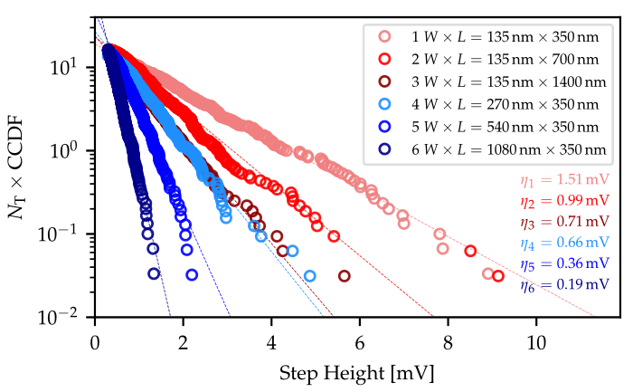
Fig. 1: Exponential distributions of individual charge ΔVth step heights for a consistent device sample set under varied VB conditions. RBB shows a heightened variance (elevated η), whereas the FBB exhibits a diminished variance (lower η).
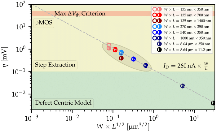
Fig. 2: The average step heights induced by single defects (η) normalized by the area (A) against the VB for pMOS devices. The impact of VB is similar for all geometries.
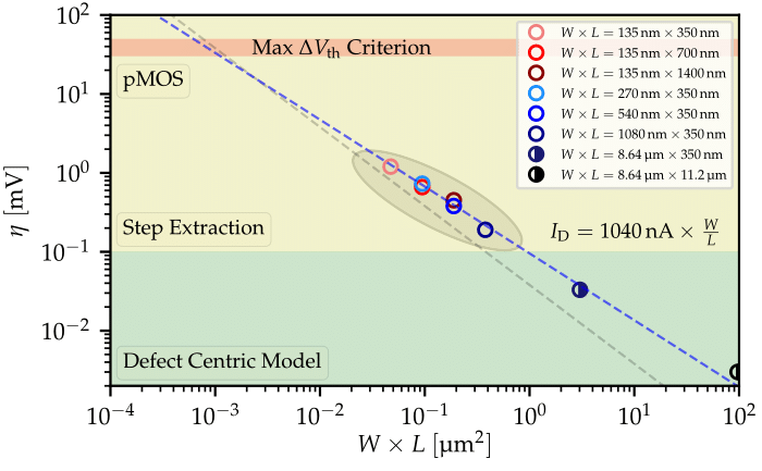
Fig. 3: TDDS on two different BB settings on a single device showing a heavy influence in the studied step height. The larger RBB leads to an increase in the step height, an observation consistent with what has been observed in the CCDFs of multiple devices.