
 |
|
||||
BiographyViktor Sverdlov received his Master of Science and PhD degrees in physics from the State University of St.Petersburg, Russia, in 1985 and 1989, respectively. From 1989 to 1999 he worked as a staff research scientist at the V.A.Fock Institute of Physics, St.Petersburg State University. During this time, he visited ICTP (Italy, 1993), the University of Geneva (Switzerland, 1993-1994), the University of Oulu (Finland,1995), the Helsinki University of Technology (Finland, 1996, 1998), the Free University of Berlin (Germany, 1997), and NORDITA (Denmark, 1998). In 1999, he became a staff research scientist at the State University of New York at Stony Brook. He joined the Institute for Microelectronics, Technische Universität Wien, in 2004 and he is currently on a tenure-track position. His scientific interests include device simulations, computational physics, solid-state physics, and nanoelectronics. |
|||||
Modeling Emerging Magnetoresistive Random Access Memories
Nonvolatile CMOS-compatible magnetoresistive random access memories (MRAMs) possess high speed and endurance as well as long retention compared to their competitors. Spin-transfer torque MMRAM (STT-MRAM) is shown to be scalable to an 8nm technology node and is considerably faster than flash memory. The main element is a magnetic tunnel junction (MTJ) composed of a CoFeB reference layer (RL) separated by an MgO tunnel barrier (TB) from a free magnetic layer (FL). In STT-MRAM, however, the write current runs through the MTJ, putting limitations on its speed and endurance. To circumvent the reliability issues and to make MRAM faster, alternative switching mechanisms are investigated. Spin-orbit torques (SOT) are extremely promising as they allow separating the write and read current paths and accelerate the switching to sub-nanosecond scale. Emerging SOT-MRAM devices are composed of multiple magnetic layers separated by tunnel barriers and non-magnetic metallic spacers. To efficiently model magnetization dynamics in complex, multilayered structures, an approach that couples the spin and charge transport is employed. Appropriate boundary conditions at the interfaces are applied to determine the spin and charge transport in metallic spin valves and magnetic tunnel junctions. We demonstrate the versatility of our approach by applying it to evaluate efficient magnetic field-assisted switching in SOT-MRAM as well as magnetic field-free magnetization control in SOT-MRAM employing noncollinear antiferromagnet Mn3Sn as shown below.
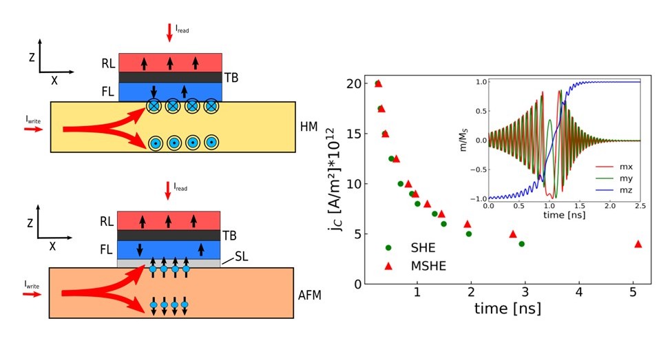
Fig. 1: Structures of a SOT-MRAM cell, with a heavy metal layer, the ferromagnetic FL, the TB, the ferromagnetic RL, and with an antiferromagnetic layer (AFM), the spaser layer (SL), the TB and the RL. The switching time for several current densities for perpendicular magnetization switching by the magnetic spin Hall effect (MSHE) and in-plane magnetization switching by the conventional spin Hall effect. Inset: The x,y, and z components of the normalized magnetization during the perpendicular magnetization switching facilitated by MSHE.