4.4 Discretization
Various authors [85, 86, 87, 88, 89] reported numeric instabilities, when directly applying the finite
volume method to Equation (4.2) using drift diffusion and thus developed various discretization
schemes for DG and developed higher resolution schemes. An almost complete list of schemes is given
in [9]. In this work only two discretization schemes, suggested by [9], will be discussed. The first
discretization is called the simplified scheme, which simply neglects the second order term in Equation
(4.2) and exhibits numeric stability. The ‘full scheme’, is the second discretization of Equation (4.2).
In this scheme Equation (4.4) is used instead of Equation (4.2). In the course of this thesis, both
schemes, have been implemented in ViennaSHE [65]. The simplified and full scheme have
been implemented into the device simulator MinimosNT by [90]. In all implementations
convergence of the non-linear solver has been achieved without any problems for the full and the
simplified scheme. Although the simplified scheme often lead to faster convergence for the
non-linear solver, when used in a Gummel-loop with the spherical harmonics expanded
BTE.
4.4.1 The Simple Scheme
Following [9], the second order terms in Equation (4.2) are neglected yielding,
γ(x,t) =  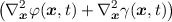 , , | | (4.17) |
in a homogeneous semiconductor. Directly applying a finite volume discretization gives
where V i is the volume of the box around vertex i, Aij are the interfaces and dij are the
distances between vertices i and j. Additionally it has been assumed that the semiconductor is
homogeneous.
4.4.2 The Full Scheme
In the full scheme, Equation (4.2) is replaced by Equation (4.4). Thus the equations for electrons and
holes to be discretized are
| γp(x,t) | = -  , , | (4.19)
|
| γn(x,t) | =   . . | (4.20) |
Applying the finite volume method yields
| γn,i | = -  ∑
j ∑
j  , , | (4.21)
|
| γp,i | =   ∑
j ∑
j  , , | (4.22) |
which can result in convergence problems, since changes in the electrostatic potential result in
exponential changes in the charge carrier concentrations. To mitigate this one can approximate the
charge carrier concentrations using Boltzmann statistics and thus obtains
| γn,i | = -  ∑
j ∑
j 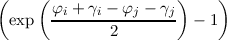 , , | (4.23)
|
| γp,i | =   ∑
j ∑
j 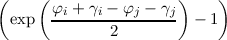 , , | (4.24) |
where it was assumed that the semiconductor is homogeneous.

 ∑
j
∑
j
 ,
,