5.2 Random Discrete Traps
Recent studies have demonstrated that in modern deca-nanometer devices the variability due to
random discrete dopants (RDD) and oxide defects has become critical in the context of reliability
[100, 101, 102, 103]. For instance, discrete charges in the oxide or at the interface lead to the
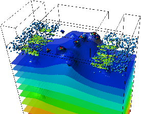
occurrence of potentially huge ΔVth shifts due to the non-uniform current flow in the channel (Figure
5.10). RDD needs to be considered when investigating the ‘step heights’ in the drain current and
threshold voltage observed in field effect devices under bias temperature or hot carrier stress. Most
studies have considered either fixed positive/negative charges or described charge capture into a
fixed number of defects by standard SRH trapping kinetics [104], where the goal is to
explain the statistical distribution of ΔVth shifts in an ensemble of devices (cf. Figure
5.9).
In this section the mere electrostatic effects of random discrete charges (traps) and random
dopants on the drain current are discussed. A discussion on the actual number of available
defects in a time-dependent manner and their activation process itself is delayed to Chapter
6.
5.2.1 Single Trap
The effect of a single charged oxide defect on the drain current in a MOSFET can be
explained without considering the time dependence of its occupancy and has been studied in
depth using a first-order quantum corrected drift diffusion model [103]. Depending on
the spatial location of the trap the resulting ΔVth, that is its ‘step height’, varies. In the
course of this thesis, together with the author of [90], this was investigated for planar
devices.
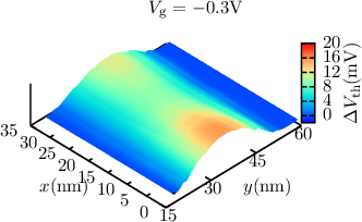
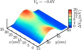
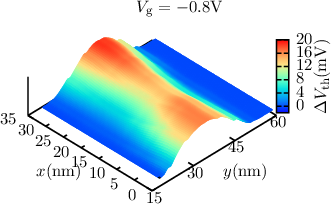
In order to obtain the spatial dependence of the ΔVth for a single defect for a single microscopic
device (constant dopant configuration), first a discrete random dopant configuration is determined
(cf. Section 5.1.1) for the planar MOSFET under investigation. Then for each position of a
single discrete elementary oxide charge in a predefined grid a single device simulation is
carried out to determine the Id - Vgcurve. At last these Id - Vgcurves are compared to the
Id - Vgcurve for the device without any oxide charges. In Figure 5.11 the ΔVth maps for a
planar p-channel MOS, with a channel doping of ND = 1018cm-3, a channel length and
width of 35nm and an effective oxide thickness (EOT) of 1nm silicon-dioxide are shown.
The ΔVth maps are a practical tool to show the trap position dependence of the ΔVth caused by a
single elementary charge, however they are not suitable to compare simulation and measurement. For
this the cumulative distribution function, obtained by considering a statistical representative ensemble
of devices, of the individual step heights is used. In order to obtain the cumulative distribution
of the step-heights of a statistically representative sample of microscopic devices has to
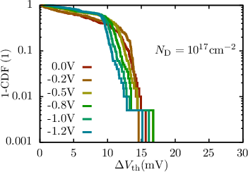
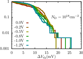
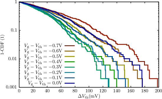
be simulated. In Figure 5.12 the cumulative distribution function of the ‘step heights’
for a single trap in a p-channel MOSFET is plotted. From the plot the dependence of
the step-height maximum on gate bias and channel doping is clearly visible. Figure 5.13
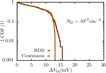
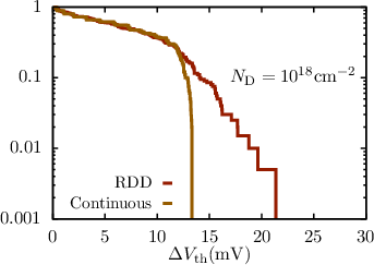
finally shows that in order to describe the occurrence of large steps in Vth a microscopic
description of the doping is necessary by comparing the CDFs for RDD and continuous doping.
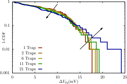
5.2.2 Multiple Traps
In real devices there are often a number of oxide traps. In sub-deca micrometer devices the oxide
volumes are so small that only a few traps, if any, can be observed in a single device [105]. When
considering multiple traps and RDD the question arises whether or not two discrete traps have an
influence on the ΔVth caused by one another [4]. It was found by [106] that two or more traps act
independent of each other, at least electrostatically. The CDFs of ΔVth for multiple traps are
comparatively plotted in Figure 5.14.
5.2.3 Mobility
Comparing simulation data (DG and DD), to measurement data it was observed that the doping
dependent mobility model needs to be slightly adjusted. Most authors have used constant
homogeneous mobilities in their random dopant studies, see for example [107]. It was later found in
[98, 108] through classical Monte Carlo simulations that random discrete dopants not only cause
potential fluctuations, but also spatial fluctuations in the scattering rates. For moments
based charge transport models it was shown by [109] that it is sufficient to adjust the
doping dependent mobility model parameters such that the bulk-mobility of a resistor
is the same when simulated with continuous and discrete doping. In the course of this
thesis it was found that this is not quite correct. It is possible to reproduce measured
mean and standard deviation in Vth due to random discrete dopants only [110]. However,
it was found impossible to reproduce measurements taken on an ensemble of p-channel
MOSFETs by simulation with quantum corrected drift diffusion taking into account discrete
traps and random discrete dopants. The devices were p-channel MOSFET with a channel
doping of ND = 1018cm-3 produced by imec. The measurements have been taken with
great care to ensure that only a single trap is created per device. The microscopic device
for simulation was calibrated to the mean Id - Vgcurve of the undegraded imec devices.
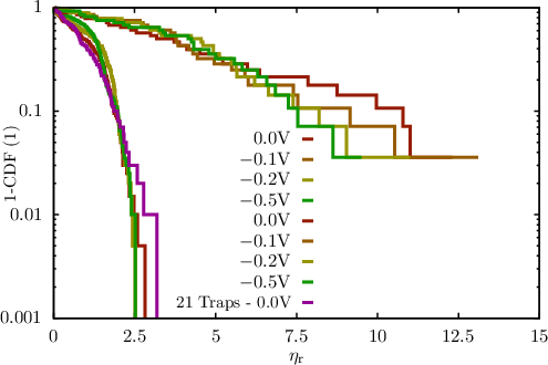
From both sets of data, namely measurement and simulation, the cumulative distribution
functions of distinct step heights are shown in Figure 5.15. To highlight the amplification of
the defect impact due to the random dopants and to be able to compare MOSFETs of
slightly different geometries, we normalize the step height by the theoretical value obtained
through the charge-sheet approximation assuming that each trap is located directly at the
interface:
 | (5.3) |
where Cox is the nominal gate oxide capacitance. Surprisingly the simulation cannot reproduce the
measurement by a factor of 5 in ηr. This suggests that the purely electrostatic picture to
determine step heights is not entirely correct as previously reported, for example in [98].
Not even the largest step heights, caused by a single trap, can be reproduced. Large step heights
are, in the simulation, due to huge fluctuations in the potential leading to a dominant percolation,
which can be ‘blocked’ by a single trap causing a huge step in drain current. Recalling that ΔVth is
estimated by comparing Id -Vgcurves or by calculating ΔVth from measured steps in the drain current
ΔId by a SPICE level 1 model [111], the only parameter that has not been accounted for is charge
carrier mobility μ. As stated initially, in [98] it was shown that a quantum corrected drift
diffusion simulation underestimates the standard deviation in current fluctuations caused by
random discrete dopants or random discrete charges by at least 20%, when compared to
solutions obtained from a calibrated Monte Carlo simulator incorporating RDD. Thus
deviations seen in Figure 5.15 can be minimized by incorporating fluctuations in mobility on a
macroscopic level or ionized impurity scattering on a microscopic level. This deviation
of 20% explains the difference between measurement and simulation using DD and DG
models.
 C
C B
B D
D