6.1 Measurement Techniques
For an explanation of many BTI experiments it is instructive to introduce one often employed basic
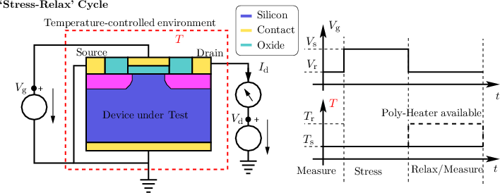
element of a BTI experiment first. In this work this basic element is termed a single ‘stress-relax’ cycle
for BTI (cf. Figure 6.2). Before the experiment starts, the fresh device is characterized by measuring
the Id -Vg, Id -Vd or capacitance-voltage curves, while taking great care not to significantly change
the device characteristics by prematurely BTI stressing the device. However, stressing the pristine
device in this inital characterisation stage is often unavoidable. For the experiment itself the drain
voltage Vd is often regulated to be as small as possible to guarantee low field conditions. Nevertheless,
constraints imposed by the measurement setup often require a higher Vd, to for example,
minimise noise in the measurement data. Whenever one is assesing homogenous BTI and not
interested in the Vth shift either during stress or relaxation, then Vd is often chosen to be at
zero volts during the respective phase. While the gate voltage Vg is precisely controlled to
cycle between stress and relaxation, the drain current can be recorded to measure the
threshold voltage deviation ΔVth. If a fast heater, such as a poly-heater device [121], is
available it is also possible to cycle the temperature in the same fashion. In a setup where the
temperature can be cycled, the device temperature during stress Ts is usually much lower
than the relaxation temperature Tr. The relaxation gate voltage V r is normally chosen
to be equal to the nominal threshold voltage V th0. Next the gate voltage is set to the
stress value, where V s normally corresponds to strong inversion for a well defined time
ts (stress). After bias temperature stress the gate voltage is, ideally instantly, set back
to its relaxation value (relax/measurement) and kept there for a given time tr until the
experiment ends. During this stress-relax cycle the drain current is recorded and compared to
the inital measurement taken before the experiment. Due to the fast transient nature of
BTI often a logarithmic time-stepping in the recording of the drain current is chosen to
capture the transient behavior of the drain current right after bias or temperature changes.
Additionally, most often one is restricted by the measurement range and bandwidth of the
equipment and can only measure the drain current over the recovery time (recovery trace).
In this work, BTI is defined as the set of gate voltages Vg and device temperatures T,
which cause a change in the threshold voltage Vth in a given time. Thus we define bias
temperature stress as an increase in threshold voltage |ΔVth| and drain current shift |ΔId| over
time. Relaxation is defined as a decreasing threshold voltage |ΔVth| and drain current
shift |ΔId| over time bringing the actual threshold voltage Vth closer to its nominal value
V th0.
6.1.1 Measure Stress Measure Technique
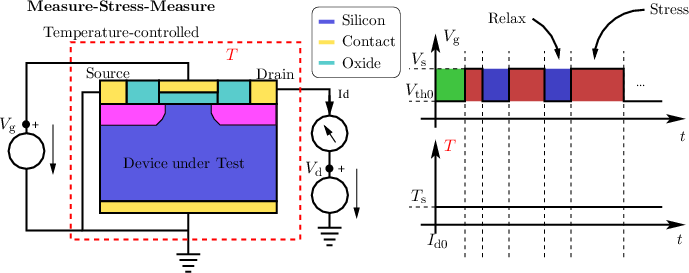
The measure stress measure (MSM) technique is a succession of multiple stress and Id -Vgmeasurement
cycles [122]. First an initial Id - Vgcurve is measured on the fresh device. Then the device is
subjected to bias temperature stress for ts seconds. Right after stress a final Id - Vgcurve is taken.
Note that during the measurement of the final Id -Vgcurve the device unavoidably relaxes. This cycle
can be repeated many times in order to measure the degradation over various stress times. In an
extended MSM measurement one records several relaxation phases after single exponentially growing
stress phases, where the device temperature is kept constant during the whole experiment. The actual
extended experiment, for bias stress, is shown in Figure 6.3. In the MSM technique the
threshold voltage shift is obtained by comparing the measured drain current at a certain gate
voltage against an initially measured Id - Vgcurve. This is possible since the gate voltage for
relaxation is chosen to be equal close to the nominal threshold voltage. Additionally, it is also a
possibility to record a fast Id - Vgcurve just before or during switching the gate voltage from
Vs to Vr. In [123] it was shown that the MSM technique is quite insensitive to mobility
changes induced by stress. Nevertheless, it was also shown that the mobility variations
induced are linearly dependent on temperature. This dependence has to be taken into
account, when comparing MSM measurements taken at different device temperatures.
6.1.2 On-the-Fly Technique
The on-the-fly (OTF) technique is a method of extracting the threshold voltage shift from the
recorded drain current with different levels of accuracy and not a separate measurement
setup. In OTF the first recorded drain current under stress conditions at a fixed drain
voltage is used as a reference to determine the threshold voltage shift. However, due to an
inherently unavoidable delay between the onset of stress and the first recorded drain current
there will always be an error in the reference drain voltage. Thus one is obliged to keep
this delay in the first measurement point as small as possible in order to minimize this
systematic error. This is also the major drawback of any OTF method. To extract the
threshold voltage shift induced by operating the device under stress conditions, usually
a SPICE Level 1 model is used [116, 124, 125]. In the simplest method (OTF1), the
drain voltage Vd and the SPICE parameter θ are assumed to be small and the effective
mobility μeff (SPICE parameter) is assumed to be constant throughout the experiment. With
these assumptions the threshold voltage shift ΔVth in the OFT1 method can be obtained
by
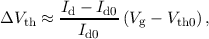 | (6.1) |
where Id0 is the reference drain current and Vth0 is the threshold voltage corresponding to Id0. Since
the OTF1 method cannot, due to the assumptions made, predict or at least compensate for mobility
changes, other OTF methods [126] have been developed. Nevertheless, all of them suffer from the
unavoidable measurement delay between stress and the first measurement point Id0. In addition, all
OTF methods also feature the inherent modelling error of the employed SPICE models to
determine ΔVth. An example of recorded stress and recovery traces using the OTF method is
shown in Figure 6.1. However, due to the inherent errors in OTF data the MSM-method
and variants thereof are often used, especially when one is only interested in the recovery
traces.
6.1.3 Direct Current Current Voltage
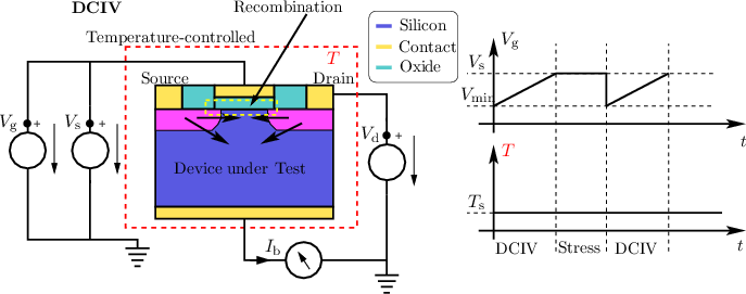
First introduced in [127] and [128], the direct-current-current-voltage (DCIV) method is used to
directly monitor the defect density by measuring the bulk current Ib, which is the result of
the carrier recombination in the oxide and at the silicon-oxide interface (cf. Figure 6.4).
In order to monitor the stress induced degradation, DCIV experiments [127, 128] are performed on
fresh devices before and after stress using a drain voltage Vd high enough to forward bias the pn
junctions. When assessing bias temperature stress, a DCIV experiment is conducted before and after
stress to compare the defect densities before and after stress.
6.1.4 Time Dependent Defect Spectroscopy
Time dependent defect spectroscopy (TDDS) is a data analysis technique to assess border traps in the
oxides of MOSFETs, where the devices need to be sufficiently small in order to be able to
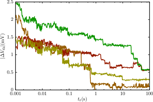
discriminate different traps [105]. Figure 6.5 shows the ΔVth recovery traces recorded after bias
temperature stress on a small area (L × W = 2μm × 160nm) n-channel MOSFET. The
only assumption TDDS does require is that the step-height and emission time of a single
defect/charge carrier trap in the oxide (cf. Chapter 4) uniquely characterizes a particular trap.
The technique itself works as follows: First a statistical significant number of subsequent
‘stress-relax’ cycles on a single device at a certain but fixed drain voltage are recorded
for a certain but fixed stress temperature. The recovery traces can then be compared by
accounting for the residual degradation from the previous relax phase. Inspecting ΔVth over
recovery time from each relaxation phase and employing the initial assumption that each
trap can be uniquely identified by a characteristic step-height one is able to calculate the
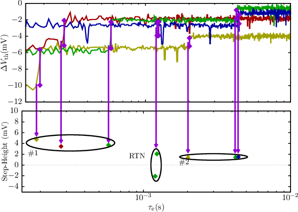
characteristic time constant, e.g. the emission time τe [129]. In Figure 6.6 the extraction
technique is illustrated. Furthermore, TDDS can be used to produce so called discrete
Capture-Emission-Time (CET) maps [29]. To this end, the TDDS method shown in Figure 6.6 is not
only applied to the recovery traces but also to the ΔVth recorded during the stress phase of
the stress-relax experiments. Then by identifying the various traps by the individual step
heights they cause it is possible to combine these two TDDS maps to a single discrete CET
map.