


Figure 8.10: Geometry of the parasitic MOSFET
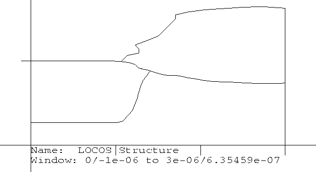
Figure 8.11: Geometry with extracted  -junction
As a second example a parasitic MOSFET resulting from the isolating oxide of a LOCOS process is presented. Fig. 8.10 shows one half of the geometry of this parasitic MOSFET. The top of the highly nonplanar oxide is covered by the gate metalization for adjacent MOS transistors. This metalization induces MOSFET-like behavior of the structure in question, although it is originally intended as an isolation between the devices.
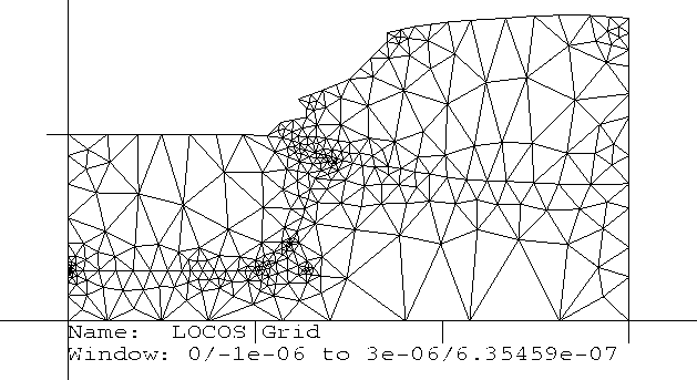
Figure 8.12: Grid generated by MESHCP
Below the oxide the silicon is lowly  -doped, and on the rear it is covered
by the bulk contact. On the left, the
-doped, and on the rear it is covered
by the bulk contact. On the left, the  -doped region with the source
contact gives rise to a -junction which can be seen in Fig. 8.11
as extracted after the MESHCP geometry preprocessing
step. Fig. 8.12 shows the initial grid generated by MESHCP, on
which the capacitance calculation is performed.
-doped region with the source
contact gives rise to a -junction which can be seen in Fig. 8.11
as extracted after the MESHCP geometry preprocessing
step. Fig. 8.12 shows the initial grid generated by MESHCP, on
which the capacitance calculation is performed.

Figure 8.13: Gate-Bulk capacitance versus gate voltage
VLSICP is run in a loop applying gate voltages from  to
to  to
create the C-V characteristics of the parasitic MOSFET in various operating
conditions. Fig. 8.13 depicts the results of this calculation, showing
a typical MOSFET input capacitance curve [Aror93][Sze81]. In the first
section, ranging up to
to
create the C-V characteristics of the parasitic MOSFET in various operating
conditions. Fig. 8.13 depicts the results of this calculation, showing
a typical MOSFET input capacitance curve [Aror93][Sze81]. In the first
section, ranging up to  , the gate-bulk capacitance is steadily decreasing
because of the increasing width of the depletion layer under the
gate. However, as the onset of inversion creates a substantial amount of
electrons at the oxide-semiconductor interface, this channel charge forms a
counter electrode to the gate capacitance. As a consequence, the capacitance
increases and finally reaches a saturation value when the device operates in
the strong inversion regime (at gate voltages of
, the gate-bulk capacitance is steadily decreasing
because of the increasing width of the depletion layer under the
gate. However, as the onset of inversion creates a substantial amount of
electrons at the oxide-semiconductor interface, this channel charge forms a
counter electrode to the gate capacitance. As a consequence, the capacitance
increases and finally reaches a saturation value when the device operates in
the strong inversion regime (at gate voltages of  and above). This
saturation value is the oxide capacitance given as
and above). This
saturation value is the oxide capacitance given as
Due to the nonplanar gate oxide, inversion will start under the left edge of
the oxide close to the source contact, where the oxide is thin. However, the
presence of charge carriers in this region will already increase the
capacitance, which is the case around approximately  gate voltage. As the
gate voltage is increased, the inversion layer will more and more extend to
the right end the symmetric axis). The threshold voltage will be reached, when
inversion occurs under the whole gate oxide. Therefore the threshold voltage
can just roughly be estimated from the capacitance curve. A value of
approximately
gate voltage. As the
gate voltage is increased, the inversion layer will more and more extend to
the right end the symmetric axis). The threshold voltage will be reached, when
inversion occurs under the whole gate oxide. Therefore the threshold voltage
can just roughly be estimated from the capacitance curve. A value of
approximately  is obtained, depending on the location under the gate,
which compares well to the results of a device simulation [Fisc94]. Since
this structure was designed as an isolating oxide, we can see that the design
goal was not met, because at gate voltages of
is obtained, depending on the location under the gate,
which compares well to the results of a device simulation [Fisc94]. Since
this structure was designed as an isolating oxide, we can see that the design
goal was not met, because at gate voltages of  the structure would no
longer isolate.
the structure would no
longer isolate.
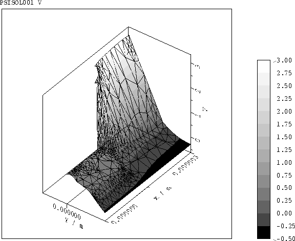
Figure 8.14: Potential distribution at  gate voltage
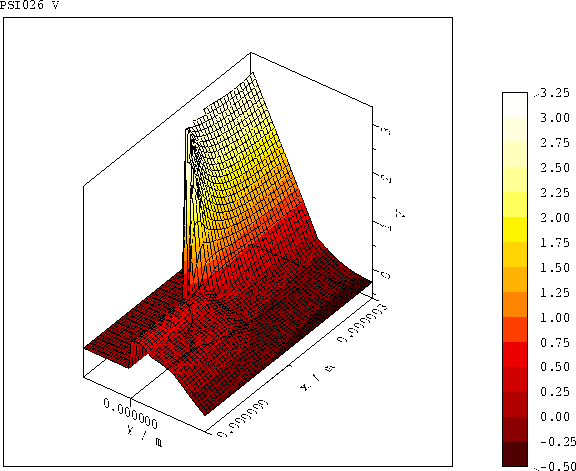
Figure 8.15: Potential distribution on vector product
grid
Fig. 8.14 and Fig. 8.15 demonstrate VLSICAP's ability to
write output on its native six-node triangular grid as well as on a tensor
product grid respectively. Both show the electrostatic potential at
a gate voltage of  . The kink at the oxide-semiconductor interface is due
to the discontinuity of the permittivity.
. The kink at the oxide-semiconductor interface is due
to the discontinuity of the permittivity.