


Next: 7.4 Thermal Analysis of
Up: 7. Simulation Results
Previous: 7.2 Five-Stage CMOS Ring
Most of the bipolar logic families such as T2L and I2L are
saturated-mode logic circuits. As the transistors are driven into saturation,
circuit speed is diminished. Several techniques have been considered to
prevent saturation such as Schottky clamping. To prevent the transistors from
saturating, the current and voltage swings have to be limited. The operation
of non-saturating logic is based on current switching and is hence known as
current mode logic (CML). A CML gate is an emitter coupled logic (ECL) gate
stripped of the emitter-follower [11] which
provided the power gain for driving external circuits. Also the gate
propagation delay is increased by the transit time of the transistor, the
overall speed is more than compensated by the reduced RC time constant that
the external load would have placed on the switching pair [71].
However, due to the improved fabrication technologies the situation is
considerably different from that in which ECL was developed and the
emitter-follower can be considered an unnecessary artifact of the past.
Figure 7.14:
Five-stage CML ring oscillator
![\begin{figure}
\begin{center}
\resizebox{16cm}{!}{
\psfrag{It}{$\scriptstyle I_{...
...ncludegraphics[width=16cm,angle=0]{figures/cml-osc.eps}}\end{center}\end{figure}](img536.gif) |
The DC transfer characteristic of a single stage without load from
Fig. 6.12 can be approximated by assuming a simple
Ebers-Moll model for the transistors [71,1]. The input
voltage is compared to the reference voltage
| Vin |
= |
 - Vref
 |
(7.8) |
| |
= |
VBE1 - VBE2 |
(7.9) |
| |
= |
VT .  ln ln - ln
- ln
 = VT .
  ln ln
 . . |
(7.10) |
Neglecting the base currents and RE, the sum of the collector currents
must be equal to the current flowing through the current source, hence
With the voltage drops at RC both
 and
and
 can be calculated as
 |
= |
- IC1 . RC = - 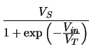 |
(7.12) |
 |
= |
- IC2 . RC = - 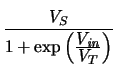 |
(7.13) |
with
The voltage gain of the single inverter is
Av =  = -
= - 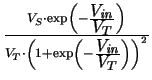 |
(7.15) |
with a maximum at
Vin = 0 V
Avmax = -  |
(7.16) |
For
Avmax greater than unity VS must be greater than
4 . VT. The larger gain is used by the system to account for static
and dynamic voltage drops that occur in practice. In practice, a minimum
gain of 4 is needed to provide sufficient noise margins [52,74].
For the simulation
VS = 20 . VT has been assumed hence a gain of
-5 could be expected. When considering an inverter chain consisting of 5
CML inverters as shown in Fig. 7.14 the total gain
occurring at the last output node is
(- 5)5 = 3125. With such a high gain,
the circuit is too sensitive to the voltage changes occurring during iteration
so no solution can be found without a proper initial-guess using conventional
techniques. However, using the shunt conductance technique with
 = 4
a DC operating point can be easily obtained with only 34 iterations.
= 4
a DC operating point can be easily obtained with only 34 iterations.
First, starting from the operating point obtained above, the DC open-loop
transfer characteristic was determined which is shown in
Fig. 7.15. The voltage gain of the circuit is shown in
Fig. 7.16 which corresponds approximately to the
simple results obtained above.
As there is no unique operating point for the closed-loop one of the node
voltages had to be fixed to force the circuit into an initial state from which
oscillations can start. Hence, the input voltage of the first inverter was
fixed to 0 V during the operating point calculation.
Figure 7.15:
Open-loop DC transfer characteristic for the CML ring oscillator.
![\begin{figure}
\vspace*{-0.5cm}
\begin{center}
\resizebox{11.4cm}{!}{
\psfrag{cm...
...cludegraphics[width=11.4cm,angle=0]{figures/cml-dc.eps}}\end{center}\end{figure}](img554.gif) |
|
Oscillations start immediately with a frequency
fDD = 6.8 GHz for DD and
fHD = 10.6 GHz for HD which
gives a relative difference of 36% for the DD model
(Fig. 7.17). This is due to the velocity overshoot which
occurs in the base-collector space charge region which cannot be modeled using
a DD transport model. The current levels are approximately equal in both
cases as shown in Fig. 7.18.
|
Figure 7.16:
Open-loop gain for the CML ring oscillator at the last three stages.
![\begin{figure}
\begin{center}
\resizebox{11.4cm}{!}{
\psfrag{5} {$\mathrm{Stage}...
...raphics[width=11.4cm,angle=0]{figures/cml-osc_gain.eps}}\end{center}\end{figure}](img555.gif) |
Figure 7.17:
Oscillation of node voltage
 of the five-stage CML ring oscillator.
Large discrepancies between DD and HD are observed.
of the five-stage CML ring oscillator.
Large discrepancies between DD and HD are observed.
![\begin{figure}
\begin{center}
\resizebox{11.4cm}{!}{
\psfrag{cml_osc_DD_new.crv:...
...egraphics[width=11.4cm,angle=0]{figures/cml_osc_V1.eps}}\end{center}\end{figure}](img556.gif) |
Figure 7.18:
Oscillation of the collector current of T1 of the five-stage CML ring oscillator.
Current levels are approximately the same for both transport models.
![\begin{figure}
\begin{center}
\resizebox{11.4cm}{!}{
\psfrag{cml_osc_DD_new.crv:...
...raphics[width=11.4cm,angle=0]{figures/cml_osc_IC1a.eps}}\end{center}\end{figure}](img557.gif) |
Next: 7.4 Thermal Analysis of
Up: 7. Simulation Results
Previous: 7.2 Five-Stage CMOS Ring
Tibor Grasser
1999-05-31