In semiconductor devices mainly two layers are made of crystalline
silicon. On the one hand the initial wafer substrate. It is produced either by
the Czochralski crystal pull method [19] or by the floating-zone crystal
growth technique [19]. Impurities (dopants) are added to the silicon in
order to set the resistivity of the wafer in a range from 0.1 ![]() cm -
50
cm -
50 ![]() cm. On the other hand often an epitaxial layer (same crystal
structure as the underlying wafer) is grown on the substrate by a high temperature
CVD process. These epitaxial layers are used to form buried layers or to
put a lightly doped layer on top of a heavily doped substrate [19].
cm. On the other hand often an epitaxial layer (same crystal
structure as the underlying wafer) is grown on the substrate by a high temperature
CVD process. These epitaxial layers are used to form buried layers or to
put a lightly doped layer on top of a heavily doped substrate [19].
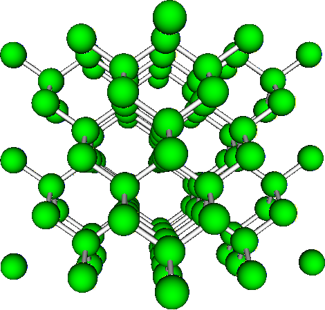
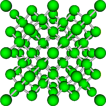
The atoms in crystalline silicon are arranged in a diamond lattice
structure with a lattice constant of 5.4307Å. Fig. 2.13 and
Fig. 2.14 show a model of the silicon crystal seen along the ![]() 110
110![]() and the
and the ![]() 100
100![]() directions [45]. Along these crystalline directions
the lattice atoms form channels with a diameter of approximately 3.3Å(0.6 of
the lattice constant) and 1.6Å(0.3 of the lattice constant). These channels
can be used by implanted ions to penetrate rather deep into the target
(channeling effect), because the scattering probability is reduced for a
particle moving along a channel.
directions [45]. Along these crystalline directions
the lattice atoms form channels with a diameter of approximately 3.3Å(0.6 of
the lattice constant) and 1.6Å(0.3 of the lattice constant). These channels
can be used by implanted ions to penetrate rather deep into the target
(channeling effect), because the scattering probability is reduced for a
particle moving along a channel.
Along a random direction, for example by tilting the wafer by 7
![]() no channel
can be recognized. Therefore these ion beam directions are preferred to generate
shallow doping profiles.
no channel
can be recognized. Therefore these ion beam directions are preferred to generate
shallow doping profiles.
The most important physical properties relevant for ion implantation are presented in Tab. 2.2 and discussed in depth in [19], [25], [66], [83].
|
![]()
![]()
![]()
![]() Previous: 2.3 Target Materials Properties
Up: 2.3 Target Materials Properties
Next: 2.3.2 Polycrystalline Silicon
Previous: 2.3 Target Materials Properties
Up: 2.3 Target Materials Properties
Next: 2.3.2 Polycrystalline Silicon