Next: 1.4 Thermal Properties and Up: 1. Introduction Previous: 1.2 The ITRS and Contents
With the same speed as integration density of semiconductor devices increases, the requirements of material properties have to be adjusted accordingly which also implies improvements of fabrication technology in terms of purity of the material sources as well as the uniform applications on reactor-scale. Hence, the fluctuation of the electrical and thermal conductivity and of the permittivity has been dramatically reduced to obtain devices with uniform characteristics and with improved reliability. Many enhancements have been proposed by former editions of the ITRS [10] and most of them have been achieved in advance. Only a few forecasted technologies are missing. Most of the missing parts are related to too high power densities or too high current densities [3]. This lack of achievements leads to more research activities and the rapid development of new types of devices and has pushed the effort to find alternative materials for device interconnect structures [19,20], dielectrics [21,22], and for the semiconductor device parts of microelectronic devices [15,23].
|
By the introduction of materials with smaller lattice constants, the number of
atomic layers slightly increases, but the possible enhancement is less than
approximately 20% due to their similar lattice constants compared to that of
![]() [24,25].
To achieve better results for down-scaling, it is necessary to introduce
materials which perform better at large thicknesses than
[24,25].
To achieve better results for down-scaling, it is necessary to introduce
materials which perform better at large thicknesses than
![]() but behave
similar to
but behave
similar to
![]() in terms of insulation and interface behavior.
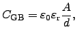
To choose the appropriate materials for a proper operation of a FET, the
value of the control capacitance between the gate and the channel must not fall
under a certain threshold value for the capacitance.
in terms of insulation and interface behavior.
To choose the appropriate materials for a proper operation of a FET, the
value of the control capacitance between the gate and the channel must not fall
under a certain threshold value for the capacitance.
The control gate capacitance
![]() can be roughly estimated by using
the formula of a capacitor for parallel plates
can be roughly estimated by using
the formula of a capacitor for parallel plates

|
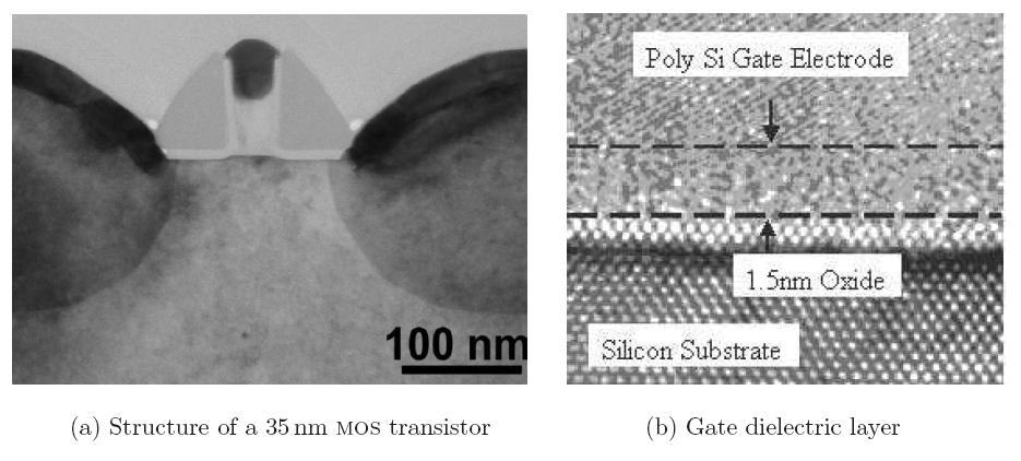
In order to increase the value of the gate capacitance, the area ![]() and the dielectric
constant
and the dielectric
constant
![]() have to be increased or the distance of the gate dielectric
layer has to be decreased. Due to technology and cost-efficient reasons, the area
has to be kept constant. The thickness of the gate dielectric layer cannot be
reduced any more due to the hard limit of the lattice
constants. The only remaining variable part in (1.1) is the material-specific
relative dielectric constant
have to be increased or the distance of the gate dielectric
layer has to be decreased. Due to technology and cost-efficient reasons, the area
has to be kept constant. The thickness of the gate dielectric layer cannot be
reduced any more due to the hard limit of the lattice
constants. The only remaining variable part in (1.1) is the material-specific
relative dielectric constant
![]() . If there exist materials which behave like
. If there exist materials which behave like
![]() but have a higher
but have a higher
![]() , the thickness of the gate dielectric can
be increased while the overall gate capacitance remains constant or increases.
, the thickness of the gate dielectric can
be increased while the overall gate capacitance remains constant or increases.
By using materials with lower dielectric constants than
![]() the
capacitance from (1.1) can be reduced as well.
This can be applied for dielectric layers in between of interconnect lines to
reduce for instance the cross-talk of these lines due to the reduced
dielectrics which are currently widely used in VLSI devices.
the
capacitance from (1.1) can be reduced as well.
This can be applied for dielectric layers in between of interconnect lines to
reduce for instance the cross-talk of these lines due to the reduced
dielectrics which are currently widely used in VLSI devices.
Another considerable performance improvement for VLSI devices was the
replacement of Al by Cu for the reduction of the specific line resistivity for
high speed applications. This material change has brought many improvements,
e.g. less power consumption due to the reduced resistivity of the interconnect
lines, but also a lot of new challenges for the device fabrication processes.
Hence, due to the higher diffusivity of
![]() , new barrier layers had to be
introduced [26]. Moreover, for special applications, where the
performance of Si-based materials is not sufficiently enough, new materials have
been investigated in order to improve the overall performance and in addition
also the reliability of these devices.
, new barrier layers had to be
introduced [26]. Moreover, for special applications, where the
performance of Si-based materials is not sufficiently enough, new materials have
been investigated in order to improve the overall performance and in addition
also the reliability of these devices.
Some these special applications are memory cells, which require high dielectric
constants in order to provide capacitances at very high package densities, so
![]() has been partially replaced by Ta compounds [27] or by
Perovskite materials1.2 [29] for capacitor materials.
has been partially replaced by Ta compounds [27] or by
Perovskite materials1.2 [29] for capacitor materials.
All these measures require a considerable effort in terms of development, time, and money. Hence, the industrial manufactures try to exploit the available technology node as long as possible to save money. This sometimes leads to quite unconventional, but very effective results in device designs [30], to new improvements in process technology [31] and material science [32].
The use of alternative materials has posed new challenges, which have to be
identified and considered as well.
For instance, the substitution of Al by Cu has increased the
conductivity and decreased bulk electromigration and therefore the long-life
reliability, but due to technology reasons, parasitic side effects occur at the
Cu interfaces [33]. First, Cu easily diffuses into
![]() and
and
![]() [34,35,26]. Therefore, a new barrier layer
has to be introduced into the device structure. Moreover, the adhesion between
[34,35,26]. Therefore, a new barrier layer
has to be introduced into the device structure. Moreover, the adhesion between
![]() and the barrier layer is quite weak, which causes a high disorder
of the crystal lattice structure at the side walls of the metal lines. Hence,
high-speed diffusion paths have been established and the desired enhancement of
the long-life reliability is not as high as estimated at the
introduction of this technology [36].
and the barrier layer is quite weak, which causes a high disorder
of the crystal lattice structure at the side walls of the metal lines. Hence,
high-speed diffusion paths have been established and the desired enhancement of
the long-life reliability is not as high as estimated at the
introduction of this technology [36].