Next: 2.3.1.2 Semiconductors as Conducting Up: 2.3.1 Interconnect Materials Previous: 2.3.1 Interconnect Materials Contents
To improve the transistor switching characteristics high current densities have to be provided by interconnect lines. Because the dimensions of the interconnect lines cannot be increased as required, the performance becomes limited by signal delays due to the transistor transfer characteristics as well as by signal delays due to the parasitic resistances, capacitances, and inductances.
One of the requirements for shrinking a technology is that the voltage and the current remain at the same order of magnitude in order to provide backward compatibility to former circuit designs. But when the current remains constant at shrinking device feature sizes the current density increases quadratically with feature size reduction.
In order to provide good conduction properties for good device characteristics, a low sheet resistivity of the interconnect lines is not sufficient. Moreover, a low contact resistivity to other parts of the device, e.g. to bonding wires, vias, and semiconductor regions, is required. The phase state of conducting materials has to be mechanically stable over a wide temperature range, which also implies that the diffusion of ions into adjacent material regions has to be negligible. This requirement is very important for narrow interconnect lines, where the diffusion of some metals provide additional trap sites in the dielectrics and additional dopants in semiconductor materials, which would result in a long-term change in the device characteristics. One of these effects is called ``contamination''. It reduces reliability and lowers the quality of the device characteristics. The second effect is called ``poisoning'', which not only reduces but can destroy the device characteristics immediately due to changes in the doping profile. However, both effects destroy the desired device characteristics if a longer period of time is considered.
To provide appropriate barrier and protective layers the compatibility of the materials has to be clarified according to the requirements of the device structures to avoid performance reductions due to mechanical and electrical material constraints. This can be done for instance by matching volume expansion coefficients. Furthermore, another serious concern related to the introduction of new materials into an existing process is the cost of ownership (COO). Since certain materials require special treatments in terms of safety for the device structures, the fabrication equipments and the environmental laws, additional costs have to be considered as well in advance. However, if there are more benefits than costs, the materials are introduced to the semiconductor device structure if the following requirements can be fulfilled [127]:
![]() has served very well for several decades as an interconnecting material
and for bonding pads.
Al shows a high conductivity but has the disadvantage that it generates a native
oxide (
has served very well for several decades as an interconnecting material
and for bonding pads.
Al shows a high conductivity but has the disadvantage that it generates a native
oxide (
![]() ), which is very stable, similar to
), which is very stable, similar to
![]() . However,
. However,
![]() is
thermally and chemically much more resistant than
is
thermally and chemically much more resistant than
![]() . Therefore,
preventing oxidation of
. Therefore,
preventing oxidation of
![]() is very important during the fabrication process.
Yet, even though the process is very well controlled, the higher demands related
to higher current densities, brought up the problem of electro-migration, which
has forced several companies to changes the interconnect base material to
is very important during the fabrication process.
Yet, even though the process is very well controlled, the higher demands related
to higher current densities, brought up the problem of electro-migration, which
has forced several companies to changes the interconnect base material to
![]() .
Bulk
.
Bulk
![]() has a much lower tendency of electro-migration than
has a much lower tendency of electro-migration than
![]() .
On the other hand, the
.
On the other hand, the
![]() integration into the technology nodes requires
more effort due to the higher diffusivities and solubility of
integration into the technology nodes requires
more effort due to the higher diffusivities and solubility of
![]() into the
standard materials used in the interconnect stack.
To prevent the diffusion of
into the
standard materials used in the interconnect stack.
To prevent the diffusion of
![]() into
into
![]() ,
,
![]() , and other materials,
additional coating and barrier layers have to be introduced.
However, the introduction of such barrier layers posed new challenging effects
that had to be overcome. The adhesion of copper on typical barrier layers is
very weak, which results in high-diffusive paths at material interfaces with
, and other materials,
additional coating and barrier layers have to be introduced.
However, the introduction of such barrier layers posed new challenging effects
that had to be overcome. The adhesion of copper on typical barrier layers is
very weak, which results in high-diffusive paths at material interfaces with
![]() .
Hence, these weak interfaces reduce the activation energy for ion diffusion
significantly, increasing the electro-migration effects and
thereby decreasing the reliability of
.
Hence, these weak interfaces reduce the activation energy for ion diffusion
significantly, increasing the electro-migration effects and
thereby decreasing the reliability of
![]() -based technology.
Due to new materials for barrier layers at material interfaces to
-based technology.
Due to new materials for barrier layers at material interfaces to
![]() , the
reliability of
, the
reliability of
![]() interconnects can be better controlled within a certain
range to meet the circuit design requirements.
interconnects can be better controlled within a certain
range to meet the circuit design requirements.
Therefore, the interconnects have protective layers around the
![]() . In
addition to this measure, the lowest layer contacting the
. In
addition to this measure, the lowest layer contacting the
![]() surface is still
made of
surface is still
made of
![]() , as known from the
, as known from the
![]() technology.
The reason for that - once again - is reliability. If
technology.
The reason for that - once again - is reliability. If
![]() diffused into the
dielectric in a higher interconnect stack level, the
diffused into the
dielectric in a higher interconnect stack level, the
![]() could contaminate and
thereby reduce the dielectric reliability in terms of resistivity, break through
voltage, and other parasitics: Nevertheless, the device structure would still be
functional.
If, e.g.,
could contaminate and
thereby reduce the dielectric reliability in terms of resistivity, break through
voltage, and other parasitics: Nevertheless, the device structure would still be
functional.
If, e.g.,
![]() atoms diffused into the
atoms diffused into the
![]() regions, a significant shift
of the threshold voltage is observed. As a result, the transistor would no
longer be working properly resulting in complete device failure.
Hence, to ensure that
regions, a significant shift
of the threshold voltage is observed. As a result, the transistor would no
longer be working properly resulting in complete device failure.
Hence, to ensure that
![]() atoms cannot contaminate the
atoms cannot contaminate the
![]() regions, the
lowest via level is made of a less contaminating material than
regions, the
lowest via level is made of a less contaminating material than
![]() .
.
| (2.127) |
| (2.131) | |||
| (2.132) |
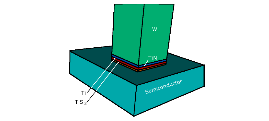
On top of the
![]() layer, a thin
layer, a thin
![]() layer is deposited that is covered by a
layer is deposited that is covered by a
![]() film. The
film. The
![]() serves as a diffusion barrier for the
serves as a diffusion barrier for the
![]() via.
In optical stacks,
via.
In optical stacks,
![]() can be used instead of
can be used instead of
![]() to reduce reflections of
light at interfaces.
to reduce reflections of
light at interfaces.
For the
![]() technology nodes, requires additional protection is required,
since the size of the
technology nodes, requires additional protection is required,
since the size of the
![]() atoms is smaller than that of
atoms is smaller than that of
![]() . Furthermore,
. Furthermore,
![]() shows a higher tendency to diffuse into the dielectrics.
The first attempt was the application of thicker layers of
shows a higher tendency to diffuse into the dielectrics.
The first attempt was the application of thicker layers of
![]() , but at the
early stages of
, but at the
early stages of
![]() technologies, the adhesion of
technologies, the adhesion of
![]() metal to
metal to
![]() was
much weaker than expected [128].
With down-scaling and increasing current densities, the weak material interface
caused too many failures, and so alternative material compounds were
investigated.
As a logical consequence,
was
much weaker than expected [128].
With down-scaling and increasing current densities, the weak material interface
caused too many failures, and so alternative material compounds were
investigated.
As a logical consequence,
![]() was replaced by other nitrates. The most
suitable of them (
was replaced by other nitrates. The most
suitable of them (
![]() ) improved interface adhesion, but was not quite
satisfactory. Hence, an additional
) improved interface adhesion, but was not quite
satisfactory. Hence, an additional
![]() layer has been introduced to the
layer has been introduced to the
![]() technology node, providing a sealing film over the
technology node, providing a sealing film over the
![]() interconnect structures. Between
interconnect structures. Between
![]() and
and
![]() , an alloy of
(
, an alloy of
(
![]()
![]() ) [33] -- due to the high-temperature phase during the
fabrication, in which both materials diffuse into each other -- builds up.
Recent arrangements have been proposed where the sealing
) [33] -- due to the high-temperature phase during the
fabrication, in which both materials diffuse into each other -- builds up.
Recent arrangements have been proposed where the sealing
![]() layer is
replaced by a
layer is
replaced by a
![]() layer only.
Compared to the high resistivity of
layer only.
Compared to the high resistivity of
![]() , the
, the
![]() layer provides the advantage
of much higher conductivity.
Hence, the
layer provides the advantage
of much higher conductivity.
Hence, the
![]() layer offers an additional conductive path, which becomes
importance for further down-scaling in interconnect structures.
The lower limit of the thickness of the
layer offers an additional conductive path, which becomes
importance for further down-scaling in interconnect structures.
The lower limit of the thickness of the
![]() layer, however, is approached.
Hence, the resistance increase in smaller interconnects is still considerable,
calling for research into alternative materials suitable for the future technology
nodes.
layer, however, is approached.
Hence, the resistance increase in smaller interconnects is still considerable,
calling for research into alternative materials suitable for the future technology
nodes.
A new approach has been reported which uses
![]() as barrier layer for
as barrier layer for
![]() interconnects [129,130].
In this case, as interconnect material
interconnects [129,130].
In this case, as interconnect material
![]()
![]() alloy is deposited. With
increasing temperatures, the
alloy is deposited. With
increasing temperatures, the
![]() grains reach their final size and shape, and
the
grains reach their final size and shape, and
the
![]() impurities accrete at material interfaces, but mostly at the
interconnect surface.
Due to diffusion and accretion processes of
impurities accrete at material interfaces, but mostly at the
interconnect surface.
Due to diffusion and accretion processes of
![]() impurities, the resulting
thickness of the
impurities, the resulting
thickness of the
![]() barrier layer is in the range of a few atomic layers
(12 to 40 Å).
Hence, this procedure offers a good alternative to the previously used
barrier layer is in the range of a few atomic layers
(12 to 40 Å).
Hence, this procedure offers a good alternative to the previously used
![]()
![]() solutions, where the thickness of the thin
solutions, where the thickness of the thin
![]() layer is limited
to 25 to 50 Å with relatively a high standard variations, compared to the
layer is limited
to 25 to 50 Å with relatively a high standard variations, compared to the
![]() layer thickness.
layer thickness.
The
![]() and the
and the
![]() technology use
technology use
![]() as etch-stop layer, where the
mechanical properties, especially the hardness of
as etch-stop layer, where the
mechanical properties, especially the hardness of
![]() , forced the technology
developers to find better materials.
In particular, a material was sought more suitable for chemical-mechanical polishing
(CMP) than
, forced the technology
developers to find better materials.
In particular, a material was sought more suitable for chemical-mechanical polishing
(CMP) than
![]() .
Because of the extreme hardness of
.
Because of the extreme hardness of
![]() , this material is well fitting to
these needs but the manufacturing process is very difficult.
On the other hand, as experiments have shown,
, this material is well fitting to
these needs but the manufacturing process is very difficult.
On the other hand, as experiments have shown,
![]() is still a good
alternative, and now used as top layer in the interlayer dielectrics (ILD)
stack even though it originally had been substituted by other alternative
materials.
The use of these new materials introduced too many problems and challenges
during the CMP process so that a return to the original material was
indicated.
With
is still a good
alternative, and now used as top layer in the interlayer dielectrics (ILD)
stack even though it originally had been substituted by other alternative
materials.
The use of these new materials introduced too many problems and challenges
during the CMP process so that a return to the original material was
indicated.
With
![]() as top ILD layer, the original technique for CMP can be
applied and the well known effects such as dishing can be considered by the same
design rules as before.
as top ILD layer, the original technique for CMP can be
applied and the well known effects such as dishing can be considered by the same
design rules as before.
 |
The requirements for the use of metals in interconnect structures can be summarized as follows:
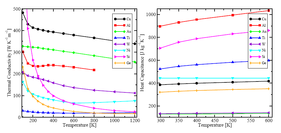
The according specific heat capacitances are presented in Figure 2.9, which shows that the tendency of the semiconductors and the different metals from Figure 2.9 is quite the similar.
However, a rigorous electro-thermal analysis, especially in the high frequency
domain, has to include electro-magnetic effects like the skin effect, which
reduces the conductivity due to a limited electro-magnetic field penetration
into the metal [145,146,147]. The penetration depth
![]() is expressed as
is expressed as