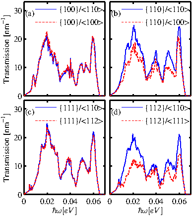
Figure 4.8 shows the transmission functions for the four surface orientations
of interest along two particular transport orientations for each case, that, as shown
below, provide the lowest and the highest thermal conductance for that particular surface.
The layer thickness in all cases is
![]() . In the case of the thin-layer with
. In the case of the thin-layer with ![]() surface orientation, in Fig. 4.8-a we consider the
surface orientation, in Fig. 4.8-a we consider the
![]() and the
and the
![]() transport channels. The transmissions of the two channels are almost the same, indicating negligible anisotropy. In the case of the thin-layer with
transport channels. The transmissions of the two channels are almost the same, indicating negligible anisotropy. In the case of the thin-layer with ![]() surface orientation, in Fig. 4.8-c we consider the
surface orientation, in Fig. 4.8-c we consider the
![]() and the
and the
![]() transport channels. Again in this case, the transmissions are almost the same.
transport channels. Again in this case, the transmissions are almost the same.
|
The transmission function of the thin-layers with ![]() and
and ![]() surfaces, on
the other hand, is orientation-dependent. For the
surfaces, on
the other hand, is orientation-dependent. For the ![]() surface thin-layers in Fig. 4.8-b, the
surface thin-layers in Fig. 4.8-b, the
![]() channel (blue line) shows the highest transmission function, and the
channel (blue line) shows the highest transmission function, and the
![]() channel (red-dotted line) the lowest. An even larger difference is observed in the case of the
channel (red-dotted line) the lowest. An even larger difference is observed in the case of the ![]() surface thin-layers in Fig. 4.8-d. The highest transmission is observed for the
surface thin-layers in Fig. 4.8-d. The highest transmission is observed for the
![]() channel (blue line), and the lowest for the
channel (blue line), and the lowest for the
![]() channel (red-dotted line). The difference in the transmission of the channels in different transport orientations is largest for energies between
channel (red-dotted line). The difference in the transmission of the channels in different transport orientations is largest for energies between
![]() for both the
for both the ![]() and the
and the ![]() thin-layers.
thin-layers.
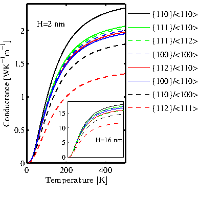
Using the transmission functions extracted from the bandstructures, the ballistic lattice thermal conductance is calculated using the Landauer formula for the thin layers with the four different surface orientations of interest. The thermal conductance as a function of the transport orientation ![]() , varying from 0 to
, varying from 0 to ![]() is shown in Fig. 4.9 for room
temperature. We calculate the conductance of thin layers for thicknesses of
is shown in Fig. 4.9 for room
temperature. We calculate the conductance of thin layers for thicknesses of ![]() ,
, ![]() ,
, ![]() and
and
![]() . With symbols the high symmetry orientations are denoted using the Miller index
notation, i.e.
. With symbols the high symmetry orientations are denoted using the Miller index
notation, i.e.
![]() - circle,
- circle,
![]() - star,
- star,
![]() - triangle, and
- triangle, and
![]() - square. These orientations are marked on the
- square. These orientations are marked on the
![]() thin-layer result in Fig. 4.9. In all cases, the conductance increases linearly as the thickness increases because the thicker layers contain more phonon modes that contribute to the thermal conductance.
thin-layer result in Fig. 4.9. In all cases, the conductance increases linearly as the thickness increases because the thicker layers contain more phonon modes that contribute to the thermal conductance.
With regards to anisotropy, for the thin-layers with ![]() surface in Fig. 4.9-a, the conductance has a maximum along the
surface in Fig. 4.9-a, the conductance has a maximum along the
![]() direction (square), and a minimum is along the
direction (square), and a minimum is along the
![]() direction (circle), although the difference is small (only
direction (circle), although the difference is small (only ![]() ). Interestingly, this observation is the same for all thicknesses considered. The conductance of the channels with
). Interestingly, this observation is the same for all thicknesses considered. The conductance of the channels with ![]() surface is shown in Fig. 4.9-b. The conductance is biggest in the
surface is shown in Fig. 4.9-b. The conductance is biggest in the
![]() transport orientation (
transport orientation ( ![]() , circle) and smallest for the
, circle) and smallest for the
![]() channels (
channels (
![]() , square). The variation between the maximum and minimum values, however, in this case is
, square). The variation between the maximum and minimum values, however, in this case is ![]() for the
for the
![]() thin layer, and decreases to
thin layer, and decreases to ![]() for the
for the
![]() layer. The conductance of channels with
layer. The conductance of channels with ![]() surface is shown in Fig.4.9-c. The conductance in this case also peaks along the
surface is shown in Fig.4.9-c. The conductance in this case also peaks along the
![]() direction (circle) and is smallest along the
direction (circle) and is smallest along the
![]() direction (triangle). The variation of the conductance with transport orientation in this case is negligible for the thinner layers, but increases to
direction (triangle). The variation of the conductance with transport orientation in this case is negligible for the thinner layers, but increases to ![]() in the
in the
![]() case. The thermal conductance for channels with
case. The thermal conductance for channels with ![]() surface is shown in Fig. 4.9-d. The maximum and minimum conductance is observed along
surface is shown in Fig. 4.9-d. The maximum and minimum conductance is observed along
![]() (circle) and
(circle) and
![]() (star), respectively. Channels with this surface orientation exhibit the largest variation in thermal conductance compared to other surfaces. The difference varies from
(star), respectively. Channels with this surface orientation exhibit the largest variation in thermal conductance compared to other surfaces. The difference varies from ![]() for the
for the
![]() layers to
layers to ![]() for the
for the
![]() layers. Overall, considering all surface and transport orientations, the maximum thermal conductance is observed for the
layers. Overall, considering all surface and transport orientations, the maximum thermal conductance is observed for the
![]() channels, and the minimum for the
channels, and the minimum for the
![]() channels. Interestingly, however, regardless of surface orientation, the thermal conductance is high in
channels. Interestingly, however, regardless of surface orientation, the thermal conductance is high in
![]() direction. This agrees well with previous works on silicon nanowires, where it is reported that the
direction. This agrees well with previous works on silicon nanowires, where it is reported that the
![]() oriented nanowires have the highest thermal conductance [111,107]. A similar conclusion was found for thin layers of larger sizes [112]. As it will be explained in next section, the phonon dispersions along the
oriented nanowires have the highest thermal conductance [111,107]. A similar conclusion was found for thin layers of larger sizes [112]. As it will be explained in next section, the phonon dispersions along the
![]() orientations are more dispersive compared to other orientations, which yield higher group velocities and, therefore, higher thermal conductance.
orientations are more dispersive compared to other orientations, which yield higher group velocities and, therefore, higher thermal conductance.

|
Figure 4.10 shows the thermal conductance of the
![]() layers as a function of temperature. For every surface orientation two transport orientations, the one
with the maximum and the one with the minimum conductance are shown (as in Fig. 4.8). The conductance increases with temperature as expected from a ballistic quantity, and starts
to saturate around
layers as a function of temperature. For every surface orientation two transport orientations, the one
with the maximum and the one with the minimum conductance are shown (as in Fig. 4.8). The conductance increases with temperature as expected from a ballistic quantity, and starts
to saturate around
![]() . The reason is that the phononic window function [57]:
. The reason is that the phononic window function [57]:
 |
(4.2) |
|