


In [111][110] the principal components of the statistical
variation of device characteristics have been identified as the variation
in device width ( ) and length (
 ), oxide thickness (
 ) and flat
band voltage (
) and flat
band voltage ( ). An inherent assumption in this variable
selection is that variation in the doping profile are not a direct source
of current variation. In other words, under manufacturing control,
profile changes resulting from fluctuation in processing conditions
do not contribute significantly to variations in
). An inherent assumption in this variable
selection is that variation in the doping profile are not a direct source
of current variation. In other words, under manufacturing control,
profile changes resulting from fluctuation in processing conditions
do not contribute significantly to variations in  and
and
 . It follows that TCAD device simulation with nominal
doping profiles can be used to predict the and
statistics by randomly selecting the input variables from known or
presumed distributions. Should this not be the case, changes in
process conditions would have to be included as statistical variables,
and the use of process simulation becomes necessary.
. It follows that TCAD device simulation with nominal
doping profiles can be used to predict the and
statistics by randomly selecting the input variables from known or
presumed distributions. Should this not be the case, changes in
process conditions would have to be included as statistical variables,
and the use of process simulation becomes necessary.
The validity of this approach is substantiated by a comparison of simulated
and experimental and distributions. The electrical test
data base collected from
production manufacturing of a 1 m CMOS process was used to
extract the experimental distributions of and
as well as the distributions of the principal statistical factors.
The simulated distributions were generated as follows:
m CMOS process was used to
extract the experimental distributions of and
as well as the distributions of the principal statistical factors.
The simulated distributions were generated as follows:
and as a function of the
principal statistical variables of each device:
Linear models provided excellent accuracy in fitting MINIMOS calculated values. The agreement was better than 1% over the parameter space region defined by the range of the input variables. The range of each variable was approximated to be equal to six times its standard deviation.
and
were generated by Monte Carlo simulation. The statistics of the
key parameters used in the simulation are listed in Table 6.1.
and variation can be modeled
by the principal statistical variables used. A TCAD worst case
characterization methodology based on these variables is presented next.
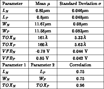
Table 6.1: Statistics of key parameters
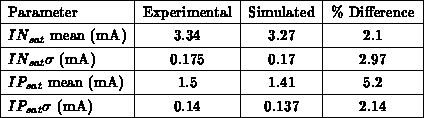
Table 6.2: Comparison of experimental and simulated and
distributions.
