


Next: 2.2 Operation Principle
Up: 2. The Photolithography Process
Previous: 2. The Photolithography Process
2.1 Some Fundamental Considerations
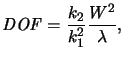
The performance of optical lithography, its limitation and possible strategies
for further enhancements can be best explained by considering the following
two figures of merit. The
resolution W, i.e., the minimal printable feature size, is given
by the expression
 |
(2.1) |
whereas the depth of focus
DOF, i.e., the range over which the
image is adequately sharp, is governed by the relation
 |
(2.2) |
In the above equations  and
NA are the actinic wavelength
and the numerical aperturea
of the exposure tool, respectively. These two quantities will be discussed in
detail throughout the subsequent sections. k1 and k2 are
characteristic constants of the specific lithography process. They are both in
the range of 0.5 to 1.0. Under special conditions they
can be theoretically calculated. The
``Rayleigh limit'' for example describes the resolving power of microscope
objectives and gives k1 = 0.61 and k2 = 1.0 [11, p. 415].
In practical semiconductor lithography, k1 and k2 generally depend on
a large number of tool, resist, and process parameters, the type of the
mask and the pattern being
imaged, as well as the requirements of the shape and allowed size range
of the developed resist profile.
and
NA are the actinic wavelength
and the numerical aperturea
of the exposure tool, respectively. These two quantities will be discussed in
detail throughout the subsequent sections. k1 and k2 are
characteristic constants of the specific lithography process. They are both in
the range of 0.5 to 1.0. Under special conditions they
can be theoretically calculated. The
``Rayleigh limit'' for example describes the resolving power of microscope
objectives and gives k1 = 0.61 and k2 = 1.0 [11, p. 415].
In practical semiconductor lithography, k1 and k2 generally depend on
a large number of tool, resist, and process parameters, the type of the
mask and the pattern being
imaged, as well as the requirements of the shape and allowed size range
of the developed resist profile.
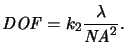
From (2.1) follows that the resolution can be
improved in three ways: by shortening the exposure wavelength  ,
by increasing the numerical aperture
NA, and by decreasing the value
of k1. As shown in Figure 2.1, all three strategies were
pursued simultaneously in the past, and are projected to continue
for the foreseeable future.
,
by increasing the numerical aperture
NA, and by decreasing the value
of k1. As shown in Figure 2.1, all three strategies were
pursued simultaneously in the past, and are projected to continue
for the foreseeable future.
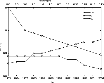
Figure 2.1:
Optical
lithography trends over the past 25 years [12], and
projected continuation over the next 10 years, illustrating
the contributions to progress from wavelength reduction [3],
increase of numerical aperture [13] and the k1
parameter [14].
|
|
At the same time as the resolution is increased by decreasing the
wavelength and increasing the numerical aperture the depth of
focus is reduced
(cf. (2.2)). The reduction in depth of focus has become
a formidable problem and has led to the development of planarization techniques
for resists like top-surface imaging or multilayer systems.
Because of the inverse square dependency on the numerical aperture,
the depth of
focus becomes extremely shallow for high-
NA tools.
The dependence on
the wavelength is less severe due to the linear relation. Eliminating
NA between (2.1) and (2.2) yields
 |
(2.3) |
which explicitly shows that for the same process parameters k1 and k2 and
the same resolution W
a shorter wavelength  gives a larger depth of focus. From the
viewpoint of the resolution, this is the motivation for exploring
shorter wavelengths, even when a longer wavelength seems to be adequate.
Another observation is that a smaller k1 increases the depth of
focus quadratically, which has motivated various
resolution enhancement techniques like advanced illumination schemes,
phase-shifting masks, and in-lens filtering. The fundamental relations
are illustrated in Figure 2.2.
gives a larger depth of focus. From the
viewpoint of the resolution, this is the motivation for exploring
shorter wavelengths, even when a longer wavelength seems to be adequate.
Another observation is that a smaller k1 increases the depth of
focus quadratically, which has motivated various
resolution enhancement techniques like advanced illumination schemes,
phase-shifting masks, and in-lens filtering. The fundamental relations
are illustrated in Figure 2.2.
Figure 2.2:
Depth of focus
DOF as a function of
numerical aperture
NA
and image resolution W, right and left figure, respectively.
For the calculation
k1 = k2 = 0.7 was chosen.
In case of diffraction limited optical lithography shorter wavelengths
provide higher depth of focus at a particular resolution.
|
|
Footnotes
- ... aperturea
- The numerical aperture
NA of a
lens is the sine of its half acceptance angle
 ,
i.e.,
NA = sin(
,
i.e.,
NA = sin( /2).
An exact definition is given in the context of aerial image
simulation in Chapter 4 on page
/2).
An exact definition is given in the context of aerial image
simulation in Chapter 4 on page ![[*]](cross_ref_motif.gif) .
.
Next: 2.2 Operation Principle
Up: 2. The Photolithography Process
Previous: 2. The Photolithography Process
Heinrich Kirchauer, Institute for Microelectronics, TU Vienna
1998-04-17
![\resizebox{14cm}{!}{
\psfrag{um}{$\mu m$ }
\psfrag{DUV_[L=193_nm]}{\scriptsize D...
...ure}{\footnotesize\textsf{Numerical aperture}}
\includegraphics{PRtradeoff.eps}}](img167.gif)