Previous: 4.1.1 Device Structure and Properties Up: 4.1 Superjunction LDMOSFET Next: 4.2 MagFET
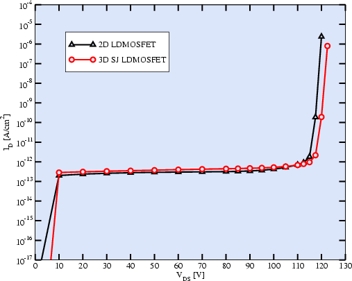
Fig. 4.3 shows the results of a breakdown simulation for the
two-dimensional LDMOSFET and the three-dimensional SJ-LDMOSFET. With both
structures a breakdown voltage of
![]() could be achieved. Since
the SJ-LDMOSFET has been designed to have a fully depleted n-drift region for
very low voltages the off-state current for low voltages is slightly higher
than for the conventional LDMOSFET.
could be achieved. Since
the SJ-LDMOSFET has been designed to have a fully depleted n-drift region for
very low voltages the off-state current for low voltages is slightly higher
than for the conventional LDMOSFET.
The n-drift doping concentration for LDMOSFET has been fixed to
![]() . Best results for the
SJ-LDMOSFET could be achieved using an asymmetric doping for the n-columns
(
. Best results for the
SJ-LDMOSFET could be achieved using an asymmetric doping for the n-columns
(
![]() ) and the p-columns
(
) and the p-columns
(
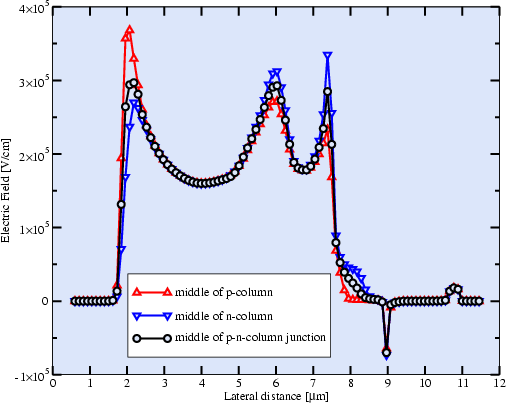
![]() ). At breakdown the
lateral electric field strength at the surface of the device is shown in
Fig. 4.4 for the middle of the p-column, at the
p-n-column junction, and the middle of the n-column. The maximum values appear
at the edges of the gate, the field plate, and the drain. At the p-n-column
junction the maximum values are almost equal. In the middle of the n- and the
p-column the maximum values appear at the gate and at the drain, respectively.
Therefore, an excellent almost constant distribution of the electric field at
the surface of the whole device could be achieved. To influence the electric
field several approaches are feasible, e.g., graded n- (higher at the drain,
lower at the gate) and p-doping (lower at the drain, higher at the gate) in the
n- and p-columns, respectively. A different idea has been proposed in
[141] using mutual tapered column widths.
). At breakdown the
lateral electric field strength at the surface of the device is shown in
Fig. 4.4 for the middle of the p-column, at the
p-n-column junction, and the middle of the n-column. The maximum values appear
at the edges of the gate, the field plate, and the drain. At the p-n-column
junction the maximum values are almost equal. In the middle of the n- and the
p-column the maximum values appear at the gate and at the drain, respectively.
Therefore, an excellent almost constant distribution of the electric field at
the surface of the whole device could be achieved. To influence the electric
field several approaches are feasible, e.g., graded n- (higher at the drain,
lower at the gate) and p-doping (lower at the drain, higher at the gate) in the
n- and p-columns, respectively. A different idea has been proposed in
[141] using mutual tapered column widths.
For the SJ-LDMOSFET an on-resistance,
![]() , which is
, which is ![]() % lower compared
to that of the LDMOSFET could be achieved (see Table 4.1).
% lower compared
to that of the LDMOSFET could be achieved (see Table 4.1).
| Device Parameter | LDMOSFET | SJ-LDMOSFET |
|
|
|
|
|
|
-- |
|
|
|
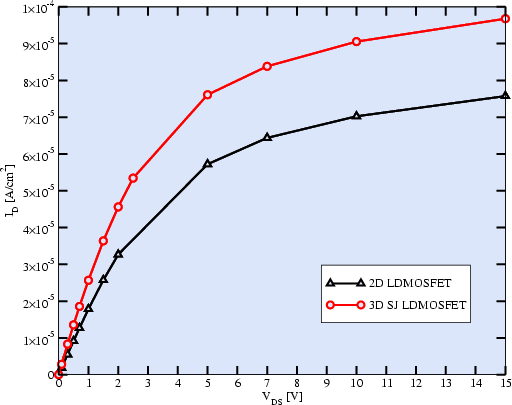
The on-state characteristics of both devices are shown in Fig. 4.5. The increased on-current of the SJ-LDMOSFET is due to the lower on-resistance of the device. Further improvement of the on-resistance can be achieved by doping engineering or by using trench gate structures [68,K6] at the expense of increased device capacitances. A different approach is shown in [142] for a structure using a folded gate to increase the channel area.
In Fig. 4.6 the contour lines of the potential distribution at breakdown are shown. The contour lines are nearly equidistantly distributed by the RESURF principle. The optimum RESURF dose could be found which depends on the n-column, p-column, and p-body doping. One can clearly see the rolling curves at the surface. Moreover, the buried oxide supports the high voltage too and dense contour lines can be observed in this area.
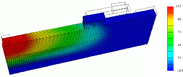
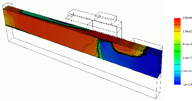
The distribution of the electron current density for the SJ-LDMOSFET is shown in Fig. 4.7. The whole current flow happens in the n-column drift region and the p-column does not contribute to the current flow. Thus, the on-resistance of the device can be further improved using a larger n-column width than the p-column width ensuring complete charge compensation in the drift region.
Robert Klima 2003-02-06