Previous: 4.3 Silicon on Insulator MOSFET Up: 4.3 Silicon on Insulator MOSFET Next: 4.3.2 Results
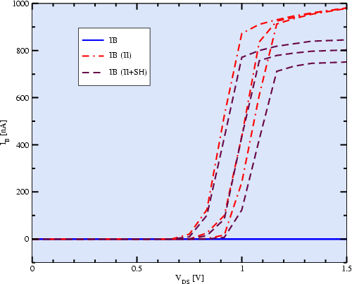
Simulation of SOI MOSFETs is challenging because the floating body region introduces a poor condition of the equation system [149,151]. Furthermore, the standard energy-transport equations [152,153,154] cannot be directly applied, because they predict unreasonable output characteristics [155]. In this work the instabilities of the equation system have been reduced by using a special iteration scheme (see Section 3.6.7): in a pre-step, the body potential was fixed to an initial value until convergence was reached. In the second step, the body potential was released until a solution was found. Using this approach, the number of required iterations could be reduced dramatically.
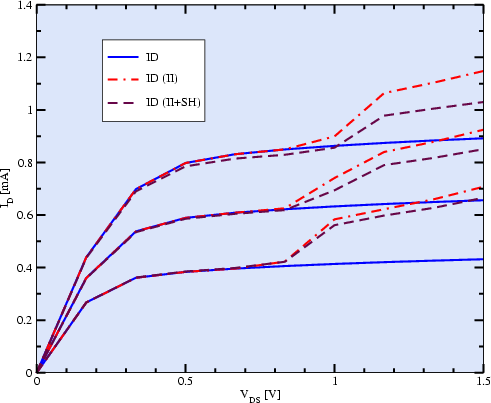 |
SOI technology offers many features, such as excellent isolation, latchup-free
operation, a high packing density, or less leakage current. The kink effect in
the output characteristic is clearly undesired as it introduces distortions in
the output signal. This issue is rather crucial for analog applications.
As shown before (see Section 4.1.1) the excess carriers
can be drained of by a bulk contact. For LDMOSFETs which are
fabricated in thick SOI layers this contact is formed using an additional
p![]() -doping in parallel to the n
-doping in parallel to the n![]() -doping at the source contact. For
devices fabricated on thin SOI layers of several ten nanometer thickness, this
approach is not applicable. Thus the body contact which is used to drain off
the excess carriers must be implemented in the third dimension.
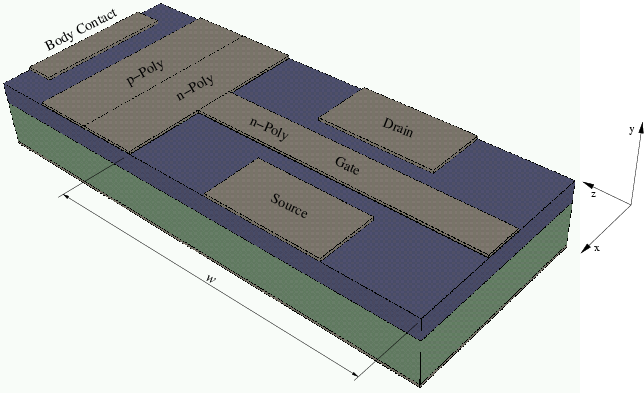
Fig. 4.14 shows the geometry of the simulated device. The
SOI layer thickness is
-doping at the source contact. For
devices fabricated on thin SOI layers of several ten nanometer thickness, this
approach is not applicable. Thus the body contact which is used to drain off
the excess carriers must be implemented in the third dimension.
Fig. 4.14 shows the geometry of the simulated device. The
SOI layer thickness is
![]() , the printed gate length is
, the printed gate length is
![]() and the device width
and the device width ![]() for the shown device is
for the shown device is
![]() .
.
 |
Robert Klima 2003-02-06