

Chapter 7 Thin Material Layer Refinement for Etching Simulations
Thin material layers are structures that commonly occur during the fabrication of semiconductor devices (e.g., LEDs or staircase patterns in 3D NAND flash memories) [31, 32]. During the fabrication of such devices, thin material films are deposited on top of the wafer, which are subsequently partially etched to create the desired device topography. Therefore, the appropriate handling of thin material layers is important to enable highly accurate process TCAD simulations of cutting edge electronic devices. The fabrication processes utilized during the fabrication of such devices (i.e., LEDs or NAND flash memories) contain multiple etching process steps. Etching processes can be simulated with Boolean operations of level-set functions, which will be discussed in Section 7.1. As long as a flat thin material layer (e.g., in the \(\si {\nano \meter }\) regime) continuously passes through the simulation domain, i.e., after the deposition of a thin material film, the level-set method is able to represent these material layers with a coarse (e.g., \(\si {\micro \meter }\)) resolution. However, when these thin material layers are etched in a subsequent process step (i.e., using Boolean operations), the low resolution of the simulation domain gets exposed and numerical artifacts manifest, such as those shown in Figure 7.1:


The relative thickness \(d\) of the thin material layers stays constant in all three depicted scenarios, whereas the grid resolution is varied. The resolution in Figure 7.1a is \(4d\), in Figure 7.1b \(2d\), and in Figure 7.1c, \(d/6\). As is shown, the effects of the numerical artifacts are reduced when the resolution of the simulation domain is increased. However, as discussed in Chapter 6, merely increasing the resolution of the simulation domain is prohibitive due to its impact on the simulation performance.
To alleviate this issue, the hierarchical grid placement algorithm presented in Section 6.2 is used. This algorithm is based on the geometric features of the zero level-set (i.e., surface curvatures). It can thus detect where a thin material layer has been etched. However, the detection of the features happens after the Boolean operation has been performed. Therefore, the entire Boolean operation has to be performed again after the newly created sub-grids have been placed. Thus, the performance of the simulation can be improved by performing the refinement before the Boolean operation is applied. Furthermore, the geometric feature based feature detection strategy does not utilize additional information about the topography available when considering etching simulations of thin material layers (e.g., the thickness of the material layers). Nevertheless, the hierarchical grid placement algorithm based on geometric features serves as a benchmark for the algorithm proposed in this chapter.
Furthermore, it is important to note that the here discussed problem cannot be solved by the wrapping layer approach presented in Section 4.3 (see Figure 4.6). The problems in the discretization of the level-set functions discussed in this chapter stem from an insufficient resolution of the simulation domain, whereas the wrapping layer approach presented in Section 4.3 prevents the formation of undesirable voids when two level-set functions are stacked on top of each other.
In Section 7.1 it is discussed how etching processes can be simulated using Boolean operations. Section 7.2 describes the newly developed thin layer refinement algorithm. First the two primary aspects of the algorithm are discussed as well as how to determine the required resolution and how to detect the material layers affected by a Boolean operation, which are then combined into the thin layer refinement algorithm. Finally, the thin layer refinement algorithms performance is benchmarked by simulating the fabrication of a single LED pixel of an LED array (Section 7.3).
Own Contributions
The contributions in this chapter are the formulation of a flagging algorithm for Boolean operations on thin material layers. Furthermore, the algorithm is able to determine a desired target resolution to properly represent the thin material layers after the simulated etching process. This work was presented at the SISPAD 2022 conference [151] and was published in a journal article in Solid-State Electronics [150].
7.1 Etching Simulations with Boolean Operations
As discussed in Section 2.3.3 a Boolean operation between two level-set functions can be interpreted as a Boolean operation between volumes. An etching simulation can be interpreted as the removal of materials from the wafer surface until a specific volume is removed. Thus, a process step that etches the wafer surface can be simulated in a level-set based simulation framework by Boolean operations between level-set functions [58].
First, a description of the volume (i.e., the material) that is removed (i.e., etched) from the wafer surface is required, which is represented by an additional level-set function \(\chi \). Figure 7.2 shows an illustration of this process. The etching process is simulated by calculating the relative complement of all level-set functions representing material layers and the level-set function \(\chi \) representing the volume removed from the wafer.

7.2 Hierarchical Grid Placement for Thin Material Layers
The algorithm for Boolean operations presented in this section determines the distance between the two closest material layers affected by the Boolean operation. This information is then further used to calculate a minimal required local resolution (\(\Delta x_{\text {tar}}\)) to prevent the artifacts shown in Figure 7.1 from forming. Suppose the resolution of the final sub-grid is not fine enough to represent the thin material layers after the Boolean operation adequately. In that case, the grid cells are flagged for refinement, and a modified version of the hierarchical grid placement algorithm presented in Section 6.2 is executed.
First the procedure used to calculate \(\Delta x_{\text {tar}}\) from the \(\phi \)-values of the level-set functions is discussed. Next, a procedure is described that is able to determine if and where a level-set function is affected by a Boolean operation with another level-set function. These two procedures are then combined to formulate the thin layer refinement algorithm.
7.2.1 Calculating the Minimal Required Resolution
To calculate \(\Delta x_{\text {tar}}\) for accurately representing a thin material layer affected by a Boolean operation, the distance to the closest other material layer (i.e., the distance between the zero level-sets) affected by the Boolean operation (\(\text {d}_{\text {closest}}\)) has to be determined. In general the distance \(d\) between two level-set functions (i.e., \(\phi \) and \(\psi \)) can be determined by utilizing the \(\phi /\psi \)-values of the level-set function at a grid point \((i,j)\) by calculating
\(\seteqnumber{0}{7.}{0}\)\begin{align} \text {d}_{(\phi _{i,j}, \psi _{i,j})} = \phi _{i,j} - \psi _{i,j}. \label {eq:calcDistBetwennLS} \end{align} An illustration of this calculation is shown in Figure 7.3.

In Section 2.3, the convention that negative \(\phi \)-values describe the inside and positive \(\phi \)-values the outside of the volume represented by the level-set function has been introduced. This convention is essential in the following considerations since the sign of two level-set functions following this convention gives information about the direction of the outward pointing normal vector of the zero level-set.
In the case that \(\text {d}_{\phi _{i,j}, \psi _{i,j}} > 0\) the level-set function \(\phi \) lies in outward normal direction of \(\psi \), in the case \(\text {d}_{\phi _{i,j}, \psi _{i,j}} < 0\) it does not. If \(\text {d}_{\phi _{i,j}, \psi _{i,j}} = 0\), the two level-set functions overlap each other in that point and are treated as if \(\phi \) does not lie in outward normal direction of \(\psi \). Only checking the distances in outward normal direction guarantees that each material layer on top of the wafer gets a distance value assigned. Figure 7.4 shows an illustration of two level-set functions and three examples of distances in outward normal direction.
Therefore, the closest distance (in outward normal direction) between a fixed level-set function \(\psi \) and all other level-set functions \(\phi ^{k \in 1..n}\) with \(\phi ^k \neq \psi \) in the domain in the grid point \((i,j)\) is calculated as follows
\(\seteqnumber{0}{7.}{1}\)\begin{align} \text {d}_{\text {closest}} = \text {min}_{\phi ^{k \in 1..n}} (\{ \text {d}_{(\phi ^k, \psi )} | \text {d}_{(\phi ^k, \psi )} > 0 \}). \label {eq:calcDClosest} \end{align}
To associate the calculated thickness of a material layer (i.e., \(\text {d}_{\text {closest}}\)) with a grid resolution, an additional parameter is required. The parameter describes the minimal number of grid points that are required to represent a single material layer (\(\text {N}_{\text {min}}\)).
By combining the thickness of a material layer with the minimal number of grid points, the minimal required resolution \(\Delta x_{\text {tar}}\) can be expressed as

\begin{align} \label {eq:RequiredResolution} \frac {\text {d}_{\text {closest}}}{\text {N}_\text {min}} = \Delta x_{\text {tar}}. \end{align}
7.2.2 Detection of Affected Material Layers
To detect if the zero level-sets of two level-set functions \(\phi \) and \(\chi \) intersect each other near a grid point \((i,j)\), the \(\phi \) and \(\chi \)-values in a star stencil \(\eta _S\) around the grid point have to be analyzed. First, the absolute \(\phi \) and \(\chi \)-values of the central grid point of the star stencil (i.e., the grid point \((i,j)\)) are examined. If both are smaller than the resolution of the currently examined sub-grid (\(\Delta x_{\text {curr}}\)), then the two level-set functions may intersect each other close to the examined grid point. However, only considering the central grid point also detects zero level-sets that run parallel to each other or are part of the wrapping layer. Thus, the other points in the star stencil have to be examined. When the signs of at least two of the \(\phi \) or \(\chi \)-values change in two coordinate directions, the two zero level-sets intersect each other near the grid point \((i,j)\). Otherwise, the two zero level-sets do not intersect each other near the grid point \((i,j)\). An illustration of two intersecting and two non-intersecting zero level-sets are shown in Figure 7.5.


7.2.3 Thin Layer Refinement Algorithm
The procedures described in Section 7.2.1 and Section 7.2.2 are now combined into the thin layer refinement algorithm, Figure 7.6 depicts a flowchart of the entire algorithm.

The algorithm starts by determining the volume that has to be removed on the base grid and calculates the respective level-set function \(\chi \). Then all level-set functions in the simulation domain intersecting the level-set function \(\chi \) are determined (see Section 7.2.2). The level-set functions with their respective grid points that identify the intersections are stored in a list.
Next, the minimal distance in outward normal direction from all zero level-sets at the intersecting grid points to all other zero level-sets is calculated. This is achieved by calculating the distances with Equation 7.1 and checking the signs of the calculated distances if they are positive (see Section 7.2.1). When the calculated distance is negative, it is disregarded, and the distance to the next level-set function is calculated. If the resolution of the currently examined grid \(\Delta x_{\text {curr}}\) is bigger than \(\Delta x_{\text {tar}}\) (see Equation 7.3), the grid points are flagged for refinement.
After all level-set functions stored in the intersection list have been processed, the hierarchical grid placement algorithm is executed (see Section 6.2). The level-set function \(\chi \) is updated accordingly to the newly placed hierarchical grids. This refinement process is repeated on the newly generated sub-grids until the maximum refinement level (i.e., \(\text {G}_{\text {ref}}\)) is reached.
In a final refinement step, the resolution required to represent the thinnest material layer properly is calculated. The refinement ratio for the final sub-grids (\(\text {F}_{\text {ref}}\)) is calculated by combining the target resolution (i.e., \(\Delta x_{\text {tar}}\)), the resolution of the current sub-grid (i.e., \(\Delta x_{\text {tar}}\)), and the refinement ratio (i.e., \(\text {R}_{\text {ratio}}\))
\(\seteqnumber{0}{7.}{3}\)\begin{align} \label {eq:RequiredRefinementLevel} \left \lceil \frac {\log (\frac {\Delta x_{\text {curr}}}{\Delta x_{\text {tar}}})}{\log (\text {R}_{\text {ratio}})} \right \rceil = \text {F}_{\text {ref}}. \end{align} Thus, the calculated resolution is used in a concluding hierarchical grid placement step.
The advantage of the refinement algorithm presented in this chapter over an algorithm based on geometrical features of the surface (see Chapter 5) is its ability to dynamically adapt the refinement based on the thickness of the material layers involved in a Boolean operation. Additionally, the knowledge about the thickness of the material layers enables the algorithm to deviate from a fixed refinement ratio.
7.3 Benchmark Example LED Pixel Fabrication
The in Section 7.2.3 presented algorithm is evaluated by simulating the fabrication of an individual LED pixel of a LED array reported in the literature [32, 152]. The simulations presented in this section have been executed with Silvaco’s Victory Process and where executed on the ICS (see Section 4.6.3).
7.3.1 Simulation Setup
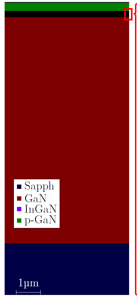
The fabrication process of an LED pixel starts by growing a \(1.9 \si {\micro \meter }\) thick \(\text {GaN}\) layer on a \((0001)\) sapphire substrate. In the next ten process steps alternating layers of \(\text {InGaN}\) and \(\text {GaN}\) with different thicknesses are deposited up to a total height of \(117.5 \si {\nano \meter }\). Afterwards, a \(\text {p-GaN}\) cap layer with a thickness of \(210 \si {\nano \meter }\) is grown on top of the structure [32, 152]. The thinnest material layer in the entire structure is a \(3 \si {\nano \meter }\) thick \(\text {InGaN}\) layer. The excess material is etched to fabricate an individual LED pixel with a diameter of \(75 \si {\micro \meter }\).
The base grid resolution of the simulation is set to \(0.125 \si {\micro \meter }\). The minimal number of grid points to represent the thinnest material layer (i.e., \(\text {N}_{\text {min}}\)) is set to \(6\). The parameters for the automatic Grid placement are \(\mathcal {E}(P) = 0.7\) and \(M = 6\). Additionally, a minimum of two grid refinement levels is presupposed (i.e., \(\text {G}_{\text {ref}} = 2\)) to guarantee an accurate description of corners in the simulation domain. The here presented simulation study focuses on the final etching step of the fabrication simulation. Evaluating Equation 7.4 with the discussed simulation parameters shows that the final sub-grid needs at least a \(256\) times finer resolution than the base-grid for an accurate representation of the thinnest material layer.
Four different configurations of the entire simulation flow are assessed in the following. To demonstrate the necessity of the previously calculated minimal required resolution, the first configuration utilizes a fixed refinement ratio \(\text {R}_{\text {ratio}}\) and a general refinement level of \(\text {G}_{\text {ref}}\) of \(3\) (4-4-4) (e.g., the finest sub-grid resolution is only \(64\) times finer than the base grid resolution). In the second and third simulation configurations, the previously calculated minimal required resolution is reached by refining the simulation domain with a general refinement level \(\text {G}_{\text {ref}}\) of \(4\) and a constant refinement ratio (4-4-4-4). These two configurations differ from each other in the chosen feature detection approach. The second configuration uses the benchmark hierarchical grid placement algorithm presented in Section 6.2 with geometric feature detection. For the third configuration the algorithm presented in Section 7.2.3 is utilized, excluding the dynamic adaptation of the grid resolution of the final sub-grid. The final configuration uses the entire algorithm presented in Section 7.2.3 utilizing a general refinement level of \(2\) with a constant refinement ratio and a concluding sub-grid with a \(16\) times finer resolution (4-4-16).
7.3.2 Discussion
Figure 7.7 depicts the entire LED device after the etching process step and zoomed-in versions of the thin material layers (active region).
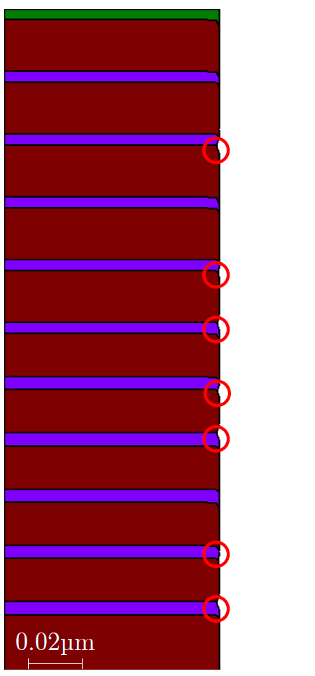
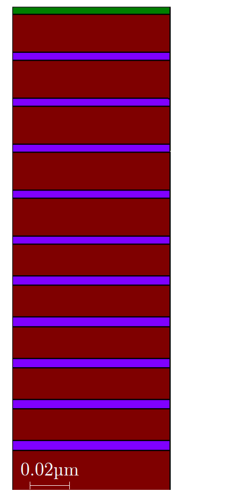
It can clearly be seen (see the visible kinks in Figure 7.7b) that using a 4-4-4 refinement is not sufficient, due to its too coarse final resolution, to properly resolve the thin \(\text {InGaN}\) material layers after the etching simulation. Thus, the following discussion focuses on refinement configurations that reach the minimum required resolution. Using the 4-4-16 and the 4-4-4-4 refinement produces the same final topography after the etching step (see Figure 7.7c).
The run-times for the etching process step are reported in Table 7.1. The simulation run with the hierarchical grid placement algorithm based on geometric features is the slowest. This is explained by the fact that it has to calculate the entire Boolean operation for each refinement level used. These observations are confirmed by the faster simulation time of the experiment using the 4-4-4-4 refinement and the in this section presented algorithm. Furthermore, when the hierarchical grid placement algorithm for Boolean operations is allowed to dynamically set the final sub-grid refinement level, it achieves a three times faster run-time than the hierarchical grid placement algorithm based on geometric features. On the one hand, this speedup is achieved by only calculating the Boolean operation once. On the other hand, this approach reduces the number of placed sub-grids since one entire grid level is skipped due to the dynamic refinement parameter.
| Feature Detection Method | Refinement Ratios | Run-Time |
| Our method | 4-4-16 | \(\SI {4}{\min }\) \(\SI {22}{\s }\) |
| Our method | 4-4-4-4 | \(\SI {8}{\min }\) \(\SI {45}{\s }\) |
| Benchmark, geometrical | 4-4-4-4 | \(\SI {11}{\min }\) \(\SI {45}{\s }\) |
7.4 Summary
A hierarchical grid placement algorithm for thin material layers affected by Boolean operations (i.e., etching simulations) has been presented. The algorithm automatically determines the thickness of the material layers affected by the Boolean operation and calculates the required refinement level based on the minimal amount of grid points that should be used to represent a material layer. The ability to consider the material layer thickness allows the algorithm to prevent the formation of numerical artifacts that occur due to an insufficient grid resolution before the Boolean operation is executed. This algorithm complements the general hierarchical grid placement algorithm presented in Section 6.2.
Moreover, the run-time of the Boolean operation is improved as a result of the ability of the algorithm to determine the minimum necessary refinement dynamically. Thus, the algorithm is able to avoid the formation of additional sub-grids. Therefore, the algorithm has a two times faster run-time when using a dynamic refinement level and a three times faster run-time than the benchmarking algorithm that utilizes geometric features of the topography for feature detection.