The delay time of a given logic block ![]() is very difficult to
quantify. It depends on the logic style, circuit techniques, the number of
inputs (fan-in) and the number of loads connected (fan-out). Compact
formulas estimating this delay for the most common logic style are
presented in [39].
is very difficult to
quantify. It depends on the logic style, circuit techniques, the number of
inputs (fan-in) and the number of loads connected (fan-out). Compact
formulas estimating this delay for the most common logic style are
presented in [39].
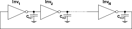
In technology development and evaluation a good method to determine the delay time is using a ring oscillator. This circuit consists of a series connection of the stages under analysis. If the stage is inverting, an odd number of them is used, and for non-inverting stages an inverter, which should be designed to present an input capacitance and delay similar to the block under analysis, is inserted into the loop.
The mostly common ring oscillator uses inverters, as shown in
Figure 4.2. If ![]() is the number of stages and
is the number of stages and ![]() the
delay time per stage, this circuit oscillates at a
frequency
the
delay time per stage, this circuit oscillates at a
frequency
![]() .
Measuring this frequency, the delay time
is calculated by
.
Measuring this frequency, the delay time
is calculated by
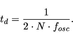
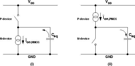
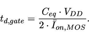
This method will be used in the next chapter to characterize the performance of the technology presented there. Inverters are also well suited to investigate the main causes of delay. If we model the inverter as in Figure 4.3 we obtain
In submicron technologies and low voltages this
equation looses validity and there are no accurate close
formulas. However, (4.7) is useful as it puts in
evidence that ![]() and
and ![]() are first order parameters.
are first order parameters.
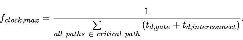
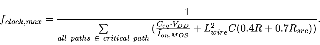
The interconnections contribute to the delay as well. This delay is caused by
loading the active devices and by distributed RC delays (especially important
for long distance lines). It means that ![]() must be the sum of the intrinsic
transistor capacitance and the parasitic capacitance of the interconnections
at that node. The distributed effect is, in general, not analytically
calculable as it depends on the geometry of the interconnections which
may have an almost arbitrary shape. As for regular shapes the capacitance and
resistance per unit length (
must be the sum of the intrinsic
transistor capacitance and the parasitic capacitance of the interconnections
at that node. The distributed effect is, in general, not analytically
calculable as it depends on the geometry of the interconnections which
may have an almost arbitrary shape. As for regular shapes the capacitance and
resistance per unit length (![]() and
and ![]() ,
respectively) are constant, and
an approximated delay can be calculated [40]:
,
respectively) are constant, and
an approximated delay can be calculated [40]:
where ![]() is the resistance of the source of signal,
is the resistance of the source of signal, ![]() the capacitance connected
to the other terminal of the line and
the capacitance connected
to the other terminal of the line and ![]() its length.
its length.
Replacing ![]() and
and
![]() in (4.5)
by (4.7) and (4.8) results
in (4.5)
by (4.7) and (4.8) results