


Next: 5.2 Application Example
Up: 5.1 Device Modeling
Previous: 5.1 Device Modeling
5.1.1 The Simulation Environment
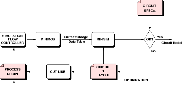
As described above, by using MINIMOS with MINISIM a link
between a device simulator and a circuit simulator without the
traditional accuracy problems of compact device models is
established. The device simulator is fully integrated in the
process flow controller of VISTA (SFC - see Section 3.2), which
in turn can read layout data (after applying a cut-line). A direct link
between layout, process simulation, device simulation and circuit
simulation is opened and a global optimization can be performed, as
depicted in Figure 5.2.
Figure 5.2:
New technology/circuit optimization.
 |
Thereupon, it is possible to investigate the influence of technology
parameters directly in the circuit performance. This is of high
importance in low-voltage, low-power circuit design, as the results of
this optimization can be much better than those following the approach of
Figure 5.1.
Rui Martins
1999-02-24