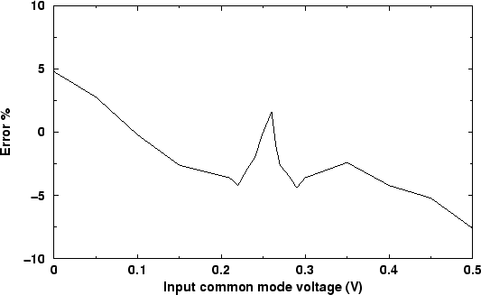
In Figure 8.10 we show the total transconductance error in the input stage (the error is normalized in relation to the transconductance when the input common mode voltage is 0.25V). It can be seen that the maximum absolute variation is within 15%, a value comparable with other designs [101][102].
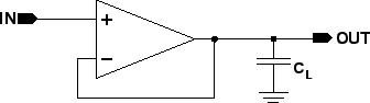
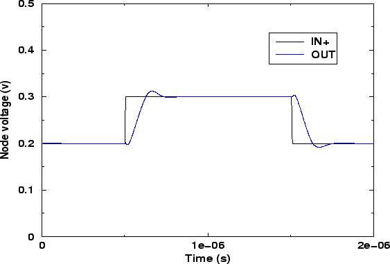
Figure 8.12 displays the transient response for small-signals for a unitary gain in a non-inverting configuration (see Figure 8.11) and with the output loaded with a 5pF capacitor. If the overshoot (9%) is too high for a specific application, it can be reduced using a higher compensation capacitor at cost of bandwidth. We opted to favor this last parameter.
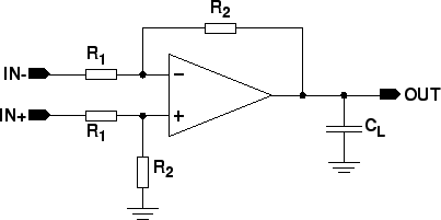
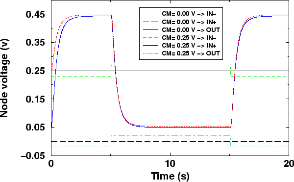
The Figure 8.14 presents the transient response as a differential amplifier (see
Figure 8.13) with a gain of ![]() for two input common mode
voltages (0.25V and 0.0V). The output was also loaded with a 5pF capacitor. As
we can see the response differences are small, only a maximum offset of
4.6mV exists, which demonstrates the efficiency of the constant
for two input common mode
voltages (0.25V and 0.0V). The output was also loaded with a 5pF capacitor. As
we can see the response differences are small, only a maximum offset of
4.6mV exists, which demonstrates the efficiency of the constant ![]() circuitry. The
mismatch in the onset are due to different initial conditions of the output voltage (that
was made equal to the common voltage) and should not be considered.
circuitry. The
mismatch in the onset are due to different initial conditions of the output voltage (that
was made equal to the common voltage) and should not be considered.
The total voltage gain is 1520 (64dB) for a 5MHz unit gain frequency. We agree that the gain is somewhat low, but this is a consequence of the reduced output resistance of transistors in these low-voltage technologies. For the time being the best choice, if gains around 60dB are too low for a given application, is to add more gain stages. In this case one must take care of the frequency stability and use more complex compensation techniques. Reference [113] is a good source for solving this problem. Other important characteristics of the operational amplifier are summarized in Table 8.3.
| Parameter | Value |
| Power supply voltage | 0.5 V |
| Input and output swing | Rail-to-rail |
| Low frequency gain | 64 dB |
| Unit-gain frequency | 5 Mhz |
| Slew-rate | 0.9 V/ |
| Total power comsumption | 15 |
| Chip area | 0.094 mm |