


Next: 2.7 Sort and Final
Up: 2. The Processing Chain
Previous: 2.5 Fabrication
2.6 Electrical Test
To evaluate the quality and stability of the semiconductor manufacturing
process a couple of electrical parameters are measured, at the stage, when the
wafers are finished with processing (fab-out). Every semiconductor factory
uses PCMs (Process Control Monitors) for this purpose. A PCM is normally positioned in the scribe line
between the integrated circuits [57]. The scribe line is the area where the
identical dies are sawed [58] before the integrated circuits are assembled in
packages. These scribe lines have a width between 150 and 60
microns and a typical length of the lithography step field
(approx 2 mm). Since the available width is very small, complicated circuitry
cannot be used inside a PCM. Normally the test structures are comprised of single
transistors, resistors, capacitors, and other passive structures.
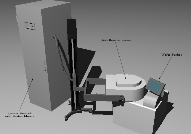
The commonly used measurement equipment for this task is a parametric tester
including an automated wafer prober for fast and automated handling.
To be able to measure the small control structures the wafer prober must be
able to use pattern recognition to align exactly on the probe pads of the
PCM structures. Furthermore, it has to move to the
structures in a fast an reliable way. Typical commercial equipment for such a
prober offer a standardized interface for control of
the wafer handling via the electrical parameter tester.
The parameter tester consists of a group of high-accuracy and fast measurement
equipment and power source units so called ``SMU'''s (Source Measure Units) which are able to measure voltage differences down to the  range
and currents in the range of picoamps [59]. Furthermore, they offer integrated
voltage and current sources which can be programmed in a very flexible
way. These SMUs can be connected to a solid-state switch matrix which wires
these instruments to a probe-card mounted in the wafer handler that connects
to the probe-pads of the PCM structures during electrical test. An overall
schematic of such an automated system is shown in Figure 2.11.
range
and currents in the range of picoamps [59]. Furthermore, they offer integrated
voltage and current sources which can be programmed in a very flexible
way. These SMUs can be connected to a solid-state switch matrix which wires
these instruments to a probe-card mounted in the wafer handler that connects
to the probe-pads of the PCM structures during electrical test. An overall
schematic of such an automated system is shown in Figure 2.11.
Figure 2.11:
An automated parameter tester including wafer
prober for final wafer acceptance test
 |
The typical wafer test steps are as follows (see Figure 2.12):
- The control computer (mainly a UNIX workstation) sends a test program to
the controller in the system cabinet through a data network connection.
- The controller converts the test information for use of the
system.
- Test data is sent to the SMU in the system cabinet.
- The SMU sends the test measurement requirements to the probe in the test
head.
- Test results are measured by the SMU or a capacitance meter.
- The results are sent through the data network connection to the control
computer for processing.
Figure 2.12:
Schematic overview of how the automated parameter tester
system performs a test
|
|
The PCM structures are measured in terms of electrical characteristics and
certain parameters are extracted for monitoring purposes. The parameters
form a hierarchy of parameter classes, depending on the importance of their
value distribution for integrated circuits. There are three classes of
parameters shown in Table 2.3.
Table 2.3:
Overview over the three different parameter classes
| Parameter |
Purpose |
Measurement Frequency |
| Class |
|
|
| Pass |
Defines if wafer material |
At least 5 PCM monitors |
| Fail |
is acceptable |
on every wafer |
| Information |
Provides additional statistical |
At least 5 PCM monitors |
| |
information on device behaviour |
on every wafer |
| Charact- |
Gives information on second |
Only a couple of times per |
| erization |
order parameters |
year on selected wafers |
|
For the class of pass/fail parameters there are defined specification
limits. These limits reflect the specifications a process technology has to
fulfil to enable competitive integrated circuit designs, e.g., if one has to
cope with a very high variation of threshold voltage of MOS transistors
one has to use big transistors to achieve a certain stability of his
design. This area consumption limits the competitiveness of the product and
therefore of the entire process technology. This constraint leads to tight
parameter limits which have to be controlled in an active way to ensure the
stability of the electrical parameters at any time. For this purpose the
Process Capability Indices (PCI) [60] are used to assess the
process' ability to achieve yield. The two most common over-all metrics to assess a
process's capability are  and
and  . These indices were created in the
Statistical Quality Control field. However, they are a useful metric even when
evaluating compensation controllers.
. These indices were created in the
Statistical Quality Control field. However, they are a useful metric even when
evaluating compensation controllers.
The following calculations assume, that the parameter values measured obey a
GAUSSIAN normal distribution function. A more detailed derivation of the
underlying central limit theorem and the characteristics of the GAUSSIAN
normal distribution and its parameters is given in Appendix A.
strictly evaluates a process's variability compared to the specification
limits on that process:
 |
(2.10) |
where USL,LSL are the upper and lower specification limits respectively and
 is the standard deviation of the normal distribution of parameter
measurement values (e.g. electrical or geometrical data like threshold voltage
or gate oxide thickness).
is the standard deviation of the normal distribution of parameter
measurement values (e.g. electrical or geometrical data like threshold voltage
or gate oxide thickness).
While also considers the mean of the process, i.e., how centered the
process is within its specification limits:
 |
(2.11) |
Where
 |
|
 |
(2.12) |
with  as the mean value of the parameter measurements.
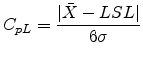
The desired values of and are commonly said to be 2.0 for a
 process. Figure 2.13 shows a graphical
representation of and with a value of 2, along with a shift in
the mean of
process. Figure 2.13 shows a graphical
representation of and with a value of 2, along with a shift in
the mean of  yielding a of 1.5.
Figure 2.13:
Example for parameter distributions and resulting and indices
|
|
Note that when the mean shifts and the variance does not, as shown in
Figure 2.13, the value remains unchanged, as also
shown in Figure 2.13. A of 2.0 means that only 2
parts per billion (ppb) are outside of the specification limits, while a value
of 1.5 means that 3.4 parts per million (ppm) will be out of
specification. These values translate to a yield of 99.9999998% and
99.99966% respectively.
These parameters are calculated for every pass/fail parameter and if one of
these parameters is below 1.0, improvement actions are undertaken (e.g. unit
process specification limits are tightened) to improve the parameter
well above 1.0.
The most common method for abnormality detection in semiconductor industry
is statistical process control (SPC) [61]. SPC is an entire
methodology, including addressing which actions to take upon detection of an
abnormality and how to inform the operators of required actions.
In traditional SPC, the expected variation is again assumed to be described by
a normal distribution occurring around a mean value. In other words, the errors
around the mean are assumed to be Identically, Independent Distributed Normal
(IID Normal). This assumption leads to the normal distribution as proven in
Appendix A. It is represented as:
where  is the measured value,
  is the mean of the distribution for
,
is the mean of the distribution for
,  is the random error in measurement of , and
 is the normal distribution with mean 0 and standard deviation
. Another form of representing the distribution of is
is the normal distribution with mean 0 and standard deviation
. Another form of representing the distribution of is
 |
(2.14) |
with
 as the normal distribution function.
In SPC an abnormality is assumed to be a shift in the mean of this
distribution (), or a change in the standard variation of the normal
distribution (). The abnormality detection technique is
based on statistics and charting of the data. Different types of statistics
have a different associated charting method. Thus, the specific fault
detection techniques are usually called XYZ chart, with XYZ denoting the
specific statistics used. Different techniques obviously test different
hypothesies. Some test whether the mean () has shifted, while
others test whether the standard deviation () has changed. Due
to the statistics, it requires a much larger sample size to detect a change in
the standard deviation than a change in the mean [62]. It is
observed, that changes in the mean are more likely to occur. Consequently,
charts to detect changes in the mean are much more common.
as the normal distribution function.
In SPC an abnormality is assumed to be a shift in the mean of this
distribution (), or a change in the standard variation of the normal
distribution (). The abnormality detection technique is
based on statistics and charting of the data. Different types of statistics
have a different associated charting method. Thus, the specific fault
detection techniques are usually called XYZ chart, with XYZ denoting the
specific statistics used. Different techniques obviously test different
hypothesies. Some test whether the mean () has shifted, while
others test whether the standard deviation () has changed. Due
to the statistics, it requires a much larger sample size to detect a change in
the standard deviation than a change in the mean [62]. It is
observed, that changes in the mean are more likely to occur. Consequently,
charts to detect changes in the mean are much more common.
The most common SPC chart is the SHEWHART Chart, also known as an XBar-R
(Average-Range) chart [63]. However in modern charting
programs this naming convention is somewhat outdated (Average, Range, Raw Data
and other statistical measures can be switched into the graph in every
possible combination).
SPC control charts show drifts and trends in the monitored
parameters. Additional control limits enable early warnings about possible
instabilities far before the parameters go out-of-spec. An example of such an
XBar-R control chart
is shown in Figure 2.14. This chart shows one of the best controlled
dimensions in semiconductor fabrication, the gate oxide thickness as a trend
graph over around 3000 measurements.
Figure 2.14:
Example for a SPC chart showing a time series of thickness
measurements of the gate oxide thickness
|
|
A second example for an SPC chart is the variation of an electrical
parameter. In Figure 2.15 the trend of the PMOS short channel
threshold is shown. This data series includes approximately 10000 measurements
over the time interval of a couple of weeks. Since this parameter is very
sensitive to the PMOS channel doping and especially also sensitive to the
thermal budget, it is much more difficult to control. The impact of corrective
actions inside the fabrication and the influence of the control limits can be
clearly seen in Figure 2.15. The control limits raise an
early warning flag and trigger corrective actions before the process gets out
of control. The jumps in the mean values indicated in Figure 2.15
indicate the impact of corrective actions in fabrication.
Figure 2.15:
Example for a SPC chart showing out-of-control events
including the impact of corrective actions for the threshold voltage of a
PMOS transistor
|
|
The second class of information parameters are measured and gathered as statistical data.
However this data is neither subject to review during the pass/fail
control mechanism nor subject to SPC methods. Examples for such parameters are
the effective channel mobility of a CMOS transistor or its effective substrate
doping.
The third class of parameters are characterization parameters which are
difficult to obtain. For this reason they cannot be monitored on a daily
basis. They are updated on annual or bi-yearly basis. Examples for such
parameters are S-parameters or temperature coefficients.
Next: 2.7 Sort and Final
Up: 2. The Processing Chain
Previous: 2.5 Fabrication
R. Minixhofer: Integrating Technology Simulation
into the Semiconductor Manufacturing Environment
![\includegraphics[origin=c,width=1.10\textwidth,clip=true]{figures/spc_tox.rot.ps}](img123.png)
![\includegraphics[origin=c,width=1.10\textwidth,clip=true]{figures/spc_vto10x05pm.rot.ps}](img124.png)
![\includegraphics[angle=0,origin=c,width=0.8\textwidth,clip=true]{figures/s600_test_flow.ps}](img105.png)
![\includegraphics[origin=c,width=1.1\textwidth,clip=true]{figures/process_capability_indices.rot.ps}](img114.png)