


Next: 2.6 Electrical Test
Up: 2. The Processing Chain
Previous: 2.4 Mask Generation
Subsections
2.5 Fabrication
In the following subsections an overview over the different process steps, a
wafer undergoes during its fabrication in the clean-room, is given.
A semiconductor manufacturing process differs markedly from other
processes. In many other types of processing plants, the material being
processed moves through the plant in a fairly simple, straightforward, and
well-integrated manner. Despite the fact that the processing flow of this
material is straightforward and linear, a flow chart depicting the process
will usually be quite complicated.
Contrast this with a semiconductor manufacturing process, which can be described
very easily with a linear processing flow chart, but whose work-in-process
(WIP) moving through the plant will follow complex paths, crisscrossing back
and forth in intricate patterns.
During wafer processing - i.e. in the semiconductor fabrication clean-room -
the integrated circuitry is formed at the surface of the single crystal
silicon wafer by numerous repetitive micro-lithographic, deposition,
diffusion, and etching steps, until it is finished. During this processing,
depending on the complexity of the technology, a set of about fifteen up
to more than thirty-five separate wafer processing cycles (which form modules
like gate module, LDD module, metal module and so on), including the
associated lithography step, were performed. An expanded flow chart of one of
these cycles appears as shown in Figure 2.8.
Figure 2.8:
Expanded flow chart of the wafer
fabrication cycle comprising one alignment step and the associated
processing
|
Here it can be seen that the wafer will iterate through this inner circle as
many times as there are masks(alignments)2.1 for adding new circuitry.
Micro-lithography is the process of defining useful shapes on the surface of a
semiconductor wafer. Typically this consists of a patterned exposure into some
sort of photosensitive material already deposited on the wafer. A variety of
processes that directly pattern the wafer are possible, such as directly
writing on the wafer with an electron beam, or nanoimprinting structures with
stamps, but at this time none is in use for high volume semiconductor
manufacturing.
The imaging basics of optical lithography have been outlined in
Section 2.4 already. Figure 2.5.2 shows the principal
components of the illumination system of a typical i-line
stepper [43] practical for structure sizes down to 350nm.
Figure 2.9:
Schematic view of the main components of the illumination
system of a lithography tool
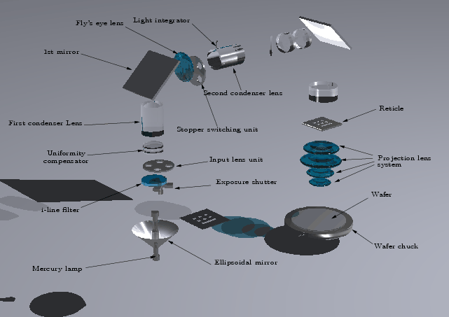 |
A detailed description of the lithography process and its modeling basics can
be found in [44].
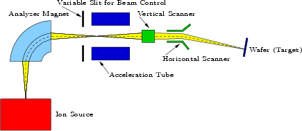
Ion implantation is a process whereby energetic dopant ions are made to
impinge on a silicon or other target, resulting in the penetration of these
ions below the target surface and thereby giving rise to controlled,
predictable dopant distributions. Low implant energy produces dopant
distributions near the surface such as are required for MOS source and drain
regions, or bipolar emitter regions. High energies produce deeply implanted
dopant profiles as required for CMOS retrograde wells and buried
layers. The provision of wafer cooling during implant allows the use of
photo resist masks to laterally control the location of dopant regions, an
inevitable feature for the production of CMOS devices. Similarly,
topographical features of the device, such as a gate stack, may be used to
impose additional masked regions to the implant, thereby allowing for the
production of cost- and yield-effective, self-aligned doping regions.
A detailed description of the physics of this process step can be found
in, e.g., [45],[46],[47],[48].
The general implanter schematic is shown in Figure 2.10.
Figure 2.10:
General schematic of an ion implantation equipment
 |
Diffusion is a key task of semiconductor wafer processing. Although
dopants are generally introduced into a wafer by ion implantation, rather than
thermally in a furnace, there is unavoidable diffusion of the dopants during
any high temperature process step. The models in this area can be categorized
into two major approaches, namely, the continuum theory of Fick's diffusion
equation and the atomistic theory.
The continuum theory requires the solution of Fick's diffusion equation,
generally with constant values for the diffusion coefficient and is adequate
for low dopant concentrations. When the doping concentrations are high, the
diffusion profiles may exhibit anomalous diffusion behavior and a simple form
of Fick's law cannot be applied, because the diffusion coefficient becomes
concentration dependent. The picture then becomes considerably more
complicated and requires an atomistic approach which studies the interactions
between native point defects (vacancies and interstitials) and dopant
atoms. The underlying idea behind all this is that the dopant atoms mostly
dissolve substitutionally in the lattice. Only through interactions with
native point defects are the dopant atoms able to jump form one site to
another, effecting long-range diffusion.
Due to the agitation of the lattice by phonons some of the defects can wander
throughout the lattice. For a simple cubic lattice this diffusion of defects
can be understood by considering the jump process between two adjacent (100)
planes, 1 and 2. If the lattice planes contain  and
and  defects per
unit surface area, respectively, and the jump rate in either direction is
given by
defects per
unit surface area, respectively, and the jump rate in either direction is
given by  then the number of defects per unit surface area jumping form
plane 1 to 2 in time
then the number of defects per unit surface area jumping form
plane 1 to 2 in time  is
is
 . For the same jump probability
in either direction, the net flux of dopants from plane 1 to 2
. For the same jump probability
in either direction, the net flux of dopants from plane 1 to 2  , can
be written as
, can
be written as
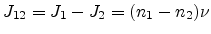 |
(2.6) |
For a small lattice constant  and assuming that the number of defects
changes slowly with distance x (continuum approximation), the above flux can be written as
and assuming that the number of defects
changes slowly with distance x (continuum approximation), the above flux can be written as
 |
(2.7) |
The defect concentration per unit volume  ,
(2.7) becomes
,
(2.7) becomes
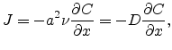 |
(2.8) |
where
 is the diffusion coefficient or diffusivity. The above
equation is Fick's first law of diffusion.
is the diffusion coefficient or diffusivity. The above
equation is Fick's first law of diffusion.
 |
(2.9) |
where  is the activation energy. is just
  , and
, and  is
proportional to the Debye frequency.
is
proportional to the Debye frequency.
A more detailed description of the theory of diffusion in semiconductors can
be found in [49],[50] and [51].
A variety of materials can be deposited by chemical vapor deposition
(CVD). Some typical materials are silicon nitride ( ), silicon dioxide
(
), silicon dioxide
( ), TEOS (
 ), polycrystalline silicon, and various
metals. Depending on the particular deposition method, the temperature varies
from about
), polycrystalline silicon, and various
metals. Depending on the particular deposition method, the temperature varies
from about
 up to
up to
 . Additionally the pressure range may vary
significantly which differentiates atmospheric pressure chemical vapor
deposition (APCVD) from low pressure chemical vapor deposition (LPCVD). A
typical characteristic of the deposition process is the deposition rate
[nm/min]. Film deposition is used to deposit other materials on top of the
silicon wafer. These materials are necessary to build functional parts of the
devices (PMOS, NMOS,Bipolar Transistor) and their interconnects in the
integrated circuit.
. Additionally the pressure range may vary
significantly which differentiates atmospheric pressure chemical vapor
deposition (APCVD) from low pressure chemical vapor deposition (LPCVD). A
typical characteristic of the deposition process is the deposition rate
[nm/min]. Film deposition is used to deposit other materials on top of the
silicon wafer. These materials are necessary to build functional parts of the
devices (PMOS, NMOS,Bipolar Transistor) and their interconnects in the
integrated circuit.
For simulation, deposition is performed by geometry operations, where the
deposition rate may vary locally. Details about different simulation
approaches for deposition can be found in [52], [53] and [54].
Etching can be subdivided into two main categories, isotropic and anisotropic etching.
This category describes etching rates which are independent of
direction. Isotropic etching is usually performed by means of wet chemistry and the
wafer is immersed into a reactive solution. The etchant species diffuses
towards the wafer surface, dissolution of the specific material takes place,
and the generated products separate in turn by diffusion from the surface [55]. The
advantages of wet etching are the possible high selectivity for specific
materials and the low damage to the substrate.
A typical anisotropic method is reactive ion etching (RIE) [56]. Here ions are
accelerated through a Chlorine- or Fluorine-based-plasma towards the wafer
surface. The Chlorine (or Fluorine) penetration into the silicon surface is
strongly enhanced by the ion bombardment. Since vertical surfaces are less
exposed to the ions, a large ratio in the etching rates can be
obtained. Furthermore (especially for deep trench etching), passivation of the
etched sidewalls is obtained by polymerization of some components of the
etching chemistry at the sidewalls. Thus only the bottom of the advancing
etching front which is exposed to the ion bombardment is free of these
polymers and, therefore, a strong anisotropy of the etched structure can be
obtained. One drawbacks of the method is the possible damage to the silicon
substrate due to the high energy of the argon ions. Furthermore, the excitation
of the plasma field with an RF electromagnetic field induces potentials in the
interconnect wires contacting e.g CMOS transistor gates and subsequently
damaging the gate oxide of the CMOS transistors (antenna effect).
Footnotes
- ... masks(alignments)2.1
- One has to carefully
distinguish between the terms ``mask'' and ``alignment''. A mask is the
physical reticle for the illumination process. An alignment is the group of
steps performed in a lithography track as shown in Figure 2.8 in
the box. The number of masks and alignments is normally not equal,
because certain reticles may be used for more than one alignment.
Next: 2.6 Electrical Test
Up: 2. The Processing Chain
Previous: 2.4 Mask Generation
R. Minixhofer: Integrating Technology Simulation
into the Semiconductor Manufacturing Environment
![\includegraphics[width=1.5\textwidth]{figures/wafer_cycle.2.ps}](img79.png)