


Next: 3.2 Overview
Up: 3. The TCAD Concept
Previous: 3. The TCAD Concept
Subsections
3.1 Introduction and State-Of-The-Art
Multiple commercially and openly available TCAD simulation tools are
available. In the following a
short overview of the history of solutions for integrating them
into a consistent work flow will be given. The following overview is far from
being complete. However the main tools are reflected.
The history of commercial TCAD began with the formation of the company Technology Modeling
Associates (TMA) in 1979. The software was a result of research performed at
Stanford University under the guidance of Professors Dutton and Plummer. The most famous
of the Stanford TCAD software programs are SUPREM and
PISCES. SUPREM3 [70], [71] is a one-dimensional process
simulator, while SUPREM4 [72], [73] can handle
two dimensions. PISCES [74], [75] is the corresponding
two-dimensional device simulator. These are general purpose simulators
designed to work with fairly arbitrary semiconductor structures. TMA's versions of
these programs were TSUPREM4 [76],[73] and
MEDICI [77],[78]. Silvaco later licensed these programs from
Stanford University too and offered a commercial alternative
(ATHENA [79],[80] and ATLAS [81]). The third major
TCAD vendor was Integrated Systems Engineering (ISE). Their equivalent product
offerings were DIOS [82] and DESSIS [83].
TMA was later acquired by Avant! which was then acquired by Synopsys.
Recently Synopsys acquired their main competitor ISE, which leaves only
Synopsys and Silvaco as the main competitors in the market. Synopsys owns now
more than 80% of the market share, which results in a market situation close
to a monopoly.
Process flow simulators are tools which simulate the full semiconductor
manufacturing flow in a certain level of detail. For special applications and
special tools (like lithography) the level of detail of the models implemented
in generic process simulators is not sufficient to cover effects like, e.g.,
simulation of proximity effects in lithography or detailed etch sidewall
shapes in plasma etching. However for the routine task of, e.g. generating a
accurate representation of a semiconductor device suitable for device
simulation the available process simulators are sufficient.
- SUPREM3 the ``mother of all process simulators'' is now
completely outdated. It is a one-dimensional process simulator incorporating
already sophisticated models like diffusion in polycrystalline layers and
point-defect diffusion.
- SUPREM4 is the basis for the two commercial tools TSUPREM4 and
ATHENA. Developed at Standford University in the group of Prof. Dutton,
it was the first consistent approach to simulate the physical behavior of
dopants in a layered two-dimensional cut through a semiconductor wafer
during semiconductor processing.
- FEDSS is based on the finite element method too. It was
developed inside IBM [84] for generating suitable device
structures for the device simulator FIELDAY [85]. It was a
fully featured process simulator. However the level of detail of especially
the diffusion models was much less sophisticated than that inside of DIOS or
SUPREM4.
- PROPHET is comparable to FEDSS and was developed in
AT&T [86]. Where the main focus was the simulation of BiCMOS
technology.
- DIOS is a two-dimensional process simulator developed initially
by the Swiss company ISE. Among the strengths is the adaptive meshing for
structures with difficult aspect ratios (e.g. smart power devices) and the
big variety of implemented models. Drawbacks are the inconsistencies in
the different granularities of the models. For instance in the diffusion
models the equilibrium diffusion parameters cannot be used as a basis for the
point-defect diffusion models.
- TSUPREM4 is a two-dimensional process simulator descendant from
the Stanford process simulator SUPREM4. Strengths are the stable and
clear programming interface and the consistent set of simulation model
parameters. A weakness is the clumsy meshing and the need
for setting up an appropriate initial mesh. Especially for automated process
split simulations it often breaks down because of an inappropriate initial
mesh.
- TAURUS-PROCESS was a very ambitious approach to implement a
process simulator based mainly on the level-set
algorithm [87], [88]. The main problem of three-dimensional process
simulation, to cope with moving internal and external three-dimensional
boundaries and especially topological changes, when certain parts or entire
layers are ``consumed'' during a semiconductor manufacturing process step,
was shifted from surface meshing to bulk meshing. However the development
failed to provide a stable three-dimensional process simulator yet.
- ATHENA is the third commercial process simulation code and an additional
descendant from SUPREM4. It is nearly identical to the TSUPREM4 simulator.
- FLOOPS is an object oriented level-set based process simulator
from the University of Florida [89]. It uses the algorithmic
language ALAGATOR to enable the implementation of new models into the
internal discretization scheme. Recently Synopsys is developing a commercial
version of FLOOPS for three-dimensional process simulation and as a successor of DIOS
Equipment simulation is still an area which is strongly under development. The
first stable equipment simulators were lithography simulators which try to
analyse the complex sequence of resist spin-on, illumination, development and
strip with finite-element methods. Equipment simulators for etching and
deposition are still strongly limited to certain manufacturing tool-sets (like
those of Applied Materials) [90],[91],[92]
and are normally not able to cover the full range of machine parameters which
can be tuned at a certain equipment. There are also no commercially available
general equipment simulators on the market.
- ILLUM2D/3D is a tool developed by the Institute for
Microelectronics at the Technical University of Vienna, which models the
full lithography process flow. It is well suited to capture the physics of
the process module like illumination. However the chemical effects during
post-exposure bake and development are not well covered by the tool.
- SPLAT/SAMPLE2D/3D are tools for aerial image simulation and
two-,three-dimensional lithography and topology simulation developed by the
University of Berkeley in the group of Prof. Neureuther [93].
- PROLITH is a fully featured lithography simulator now
distributed by KLA Tencor [94]. It offers two-dimensional and three-dimensional
functionalities and is a standard tool used by the lithography groups worldwide.
- SOLID E is the competitor to PROLITH and offers a comparable
set of features for three-dimensional lithography simulation [95].
- ACES (Anisotropic Crystalline Etch Simulation) is a
tree-dimensional etch simulator using a continuous cellular automata (CA)
model and a dynamic structure update method [96]. The program can simulate
silicon etching with different surface orientations in selected etchants
with variable etch rate ratios. It can receive two-dimensional mask designs in common
mask formats (including CIF, GDSII, BMP) and generate three-dimensional profiles in
standard solid-modeling languages.
Device simulators are the counterparts for the process simulators shown
above. However historically device simulation was done much earlier than
process simulation. Based on assumptions on the input structure of
semiconductor devices pioneering work on device simulation was carried out at
ATT [97] and IBM [98] leading to major university
efforts such as TU Vienna [99] and Stanford [100], finally
culminating in a rapid growth of TCAD vendors and development of commercial
platforms that support a broad and heterogeneous set of users.
- PISCES 2ET is a dual energy transport (for carrier
temperatures and lattice thermal diffusion) semiconductor device
simulator. Some advanced features are the simulation of the carrier and
lattice temperatures, and heterostructures in compound semiconductors. Hence,
various non-stationary phenomena such as hot carrier effects and velocity
overshoot can be analyzed using this program. The electrical behavior of
optoelectronic devices can also be simulated with reasonable accuracy. Most
of the material parameters have been calibrated and thoroughly surveyed with
the help of industry.
- FIELDAY [85] is a simulator for devices of arbitrary shape in one-
up to three-dimensions. The models are especially tailored for the analysis
of bipolar devices but field effect transistors can be modeled too. The
complementing program FEDSS is used for the generation of input structures.
- PADRE [101] is comparable to FIELDAY and an
internal development of AT&T. It is a moment based device simulator.
- MINIMOS-NT is a general-purpose semiconductor device simulator
providing steady-state, transient, and small-signal analysis of arbitrary
two- and three-dimensional device structures [102]. It was recently compared to devices
simulated with DESSIS, and it yields the same quality of results as the
commercial tool.
- MEDICI is the counterpart of TSUPREM4 on the device simulation
side. It is a pretty stable hence fairly old device simulator which can deal
with a variety of physical effects in two-dimensional semiconductor
structures. The code was licensed from Stanford University and bases entirely
on the PISCES code.
- DESSIS is a very sophisticated device simulator which deals
with two- and three-dimensional device structures. It has a fairly similar
feature list compared to MEDICI. However, it is much more stable and based on
newer source code (C++ instead of FORTRAN) than MEDICI [103].
- ATLAS is nearly identical to MEDICI in terms of features [81].
- FLOODS is the counterpart to FLOOPS on the device simulation
side [89].
Specialized device simulators work on a ``device template'' input
structure. These templates are predefined or even hardcoded in the device
simulator. The simulator assumes a certain type of device (e.g. a MOSFET for
MINIMOS [104] and PISCES [105] or a bipolar transistor for BIPOLE) and takes values for
predefined dimensions (e.g. gate oxide thickness, gate width etc.) and doping
profiles (e.g. gate channel doping profile assumed as GAUSSIAN distribution)
of the semiconductor device.
- MINIMOS is the predecessor of MINIMOS-NT. It is the famous
MOSFET device simulator which worked on an orthogonal grid generated
internally [106]. The simulator was a major breakthrough in the theoretical
investigations of semiconductor devices, because a lot of physical effects
were in reach of detailed analysis for the first time.
- PISCES is a simulator comparable to MINIMOS, developed by
Stanford University [100].
- SEQUOIA [107] device designer is a simulator comparable to MINIMOS, developed by
Sequoia Design Systems.
- BIPOLE [108],[109] is a simulator for device simulation of bipolar
transistors. The core code deals with the analysis of a one-dimensional cut
through the emitter/base/collector region of an integrated bipolar
transistor device. It adds additional parasitic elements into the analysis
like the collector resistance by analysing the geometric dimensions and
sheet resistances of the device.
The tools that define the TCAD field - process, device and circuit modeling -
have evolved steadily over the past three decades, moving from research
prototypes (both in industry and academia) towards robust workhorses that support both research and manufacturing
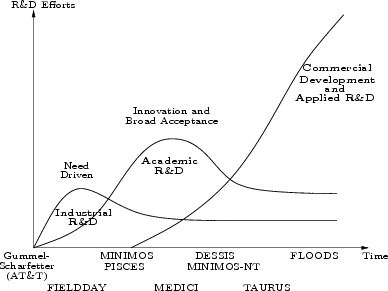
applications. Figure 3.1 shows a schematic time line of evolution
for process and device simulation. It is obvious that the development efforts of the
commercial vendors have been steadily increasing since the 80's.
Figure 3.1:
Schematic time-line of TCAD R&D for device analysis
 |
Every commercial TCAD vendor is including an environment software for
automated or at least semi-automated setup of the TCAD work flow shown in
Figure 3.2 in Section 3.2. The three workbench
software tools are GENESISE from the former ISE AG,
WORKBENCH from Synopsys Inc. and VIRTUAL WAFER FAB
from Silvaco Int.. Another free TCAD environment software is VISTA [110],[111]
from the Institute for Microelectronics, TU Vienna. However this software is not
under active development at present.
All four environments are fairly similar in their architecture. They offer
macros to schedule and generate Design of Experiments (DOE) [112]
simulation runs. For this purpose the simulator command files can be
parametrized by a special syntax which identifies the position of a dedicated
parameter in the command file. The types of parameters
supported are shown in Figure 3.6 in
Section 3.4. Furthermore, the extraction of
dedicated results from process or device simulation (values given in certain
simulation logs or result files) is supported by defining regular expressions
or output templates. However all of these environments do NOT support
interfaces from semiconductor manufacturing equipment or metrology tools. They
offer a more or less well integrated work flow for performing simulations, but
the support for interfaces from and to the simulation environment is very
little or even not implemented. In the following sections a concept is layed
out, how to set up such interfaces in a most effective and stable manner.
Next: 3.2 Overview
Up: 3. The TCAD Concept
Previous: 3. The TCAD Concept
R. Minixhofer: Integrating Technology Simulation
into the Semiconductor Manufacturing Environment