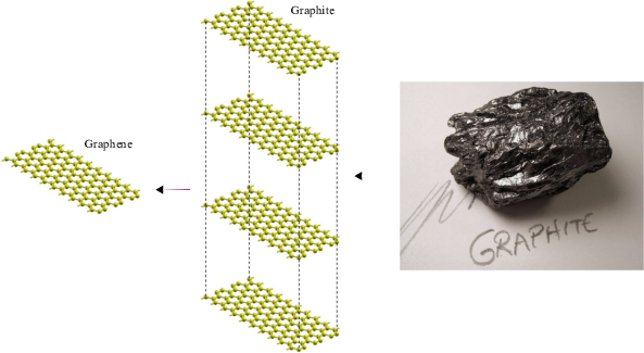
Figure 2.2: Graphene is a single layer honeycomb lattice of carbon atoms.
Graphite can be viewed as a stack of graphene layers.
In October 2004, graphene, a one-atomic layer of carbon with a honeycomb structure, started a revolution in science and technology. Physicists reported that they had prepared graphene and observed the electric field effect in their samples [24]. Shortly after, this new material attracted the attention in many areas of research including condensed matter, material physics, chemistry, and device physics. Graphene-based structures such as graphene nanoribbons (GNRs) [25], nanorods [26] quantum dots [27], and p-n junctions [28] have been successfully fabricated.
To understand graphene in more details, it is useful to consider it as the single layer limit of graphite (Fig.2.2). In this light, the extraordinary properties of honeycomb carbon are not really new. Abundant and naturally occurring, graphite has been known as a mineral for nearly 500 years. Even in the middle ages, the layered morphology and weak dispersion forces between adjacent sheets were utilized to make marking instruments, much in the same way that we use graphite in pencils today. More recently, these same properties have made graphite an ideal material for use as a dry lubricant, along with the similarly structured but more expensive compounds hexagonal boron nitride and molybdenum disulfide [29].
An extraordinarily high carrier mobility of more than 2 × 105 cm2∕Vs [30–32] makes graphene a major candidate for future electronic applications. Today a growing number of groups are successfully fabricating graphene transistors [33]. Major chip-makers are now active in graphene research and the International Technology Roadmap for Semiconductors, the strategic planning document for the semiconductor industry, considers graphene to be among the candidate materials for post-silicon electronics [34] and terahertz applications [35]. Graphene is also regarded as a pivotal material in the emerging field of spin electronics due to spin coherence even at room temperature [36,37].
One of the many interesting properties of Dirac electrons in graphene is the drastic change of the conductivity of graphene-based structures with the confinement of electrons. Structures that realize this behavior are carbon nanotubes (CNTs) and graphene nanoribbons (GNRs), which impose periodic and zero boundary conditions, respectively, on the transverse electron wave-vector. In CNT-based devices control over the chirality and diameter and thus of the associated electronic bandgap remains a major technological problem. GNRs do not suffer from this problem and are thus recognized as promising building blocks for nanoelectronic devices [38]. GNRs less than 10nm wide with ultrasmooth edges have been fabricated [39].
GNRs can be considered as a graphene sheet tailored along a certain direction and can be accordingly classified as of armchair or zigzag shape, see Fig. 2.3(a) and (b). Tight-binding calculations predict that ZGNRs are always metallic while AGNRs may be either metallic or semiconducting depending on their direction and width [40,41]. The edges of GNRs can significantly affect the electronic properties of the ribbon. In the electronic band structure of GNRs with zigzag edges a flat band, which corresponds to localized states at the edges, appears around the Fermi level [41,42]. However, such states do not appear in GNRs with armchair edges (AGNRs) [41].
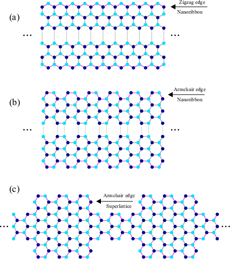
The controllable alteration of graphene by high-precision lithography [39,43,44] and chemical functionalization [45] has enabled modulation of the electronics, optical and thermal properties of these structures. A recent experimental study has reported ultra-smooth patterning of graphene nanoribbons with modulated widths which can be regarded as finite segments of GNR-based superlattices [39], see Fig. 2.3(c). Such structures can behave as multiple quantum wells and exhibit interesting quantum effects [46] such as resonant tunneling [47].
Due to possible application in nanoelectronics [38], photonics [48,49], and spintronics [50], intensive scientific research is being carried out on graphene-based structures.
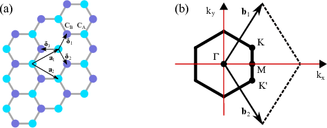
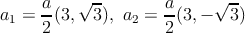
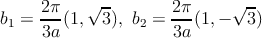
Graphene is composed of carbon atoms arranged in a hexagonal structure, as shown in Fig. 2.4. The structure can be seen as a triangular lattice with a basis of two atoms per unit cell. The lattice vectors can be written as
 | (2.1) |
where a ≈ 1.42 Å is the carbon-carbon bond length. The reciprocal lattice vectors are given by
 | (2.2) |
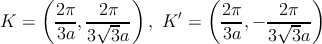
Of particular importance for the physics of graphene are the two points K and K′ at the corners of the Brillouin zone. These are named Dirac points for reasons that will become clear later. Their positions in momentum space are given by
 | (2.3) |
The three nearest-neighbor vectors in real space are
 | (2.4) |
while the six second-nearest neighbors are located at δ′1 = ±a1, δ′2 = ±a2, δ′3 = ±(a2 - a1). The tight-binding Hamiltonian for electrons in graphene considering that electrons can hop to both nearest- and next-nearest-neighbor atoms has the form (we use units such that ℏ = 1)
 | (2.5) |
where aσ,i annihilates an electron with spin σ (σ =↑,↓) and aσ,i† creates an electron with spin σ on site Ri on sublattice A. An equivalent definition is used for sublattice B. The nearest-neighbor hopping energy between different sublattices is t ≈ 2.7 eV, and t′ is the next nearest-neighbor hopping energy in the same sublattice. The value of t′ is not well known but ab initio calculations [51] indicate 0.02t ≲ t′≲ 0.2t depending on the tight-binding parametrization. These calculations also include the effect of third-nearest-neighbors hopping, which has a hopping parameter of around 0.07 eV. A tight-binding fit to cyclotron resonance experiments [52] gives t′≈ 0.1 eV.
The two-dimensional energy dispersion relations of graphene can be calculated by solving the eigen-value problem for the Hamiltonian. In the Slater-Koster scheme [53] one gets
![[ 0 f(k) ]
H = * ,
- f (k) 0](diss40x.png) | (2.6) |
where
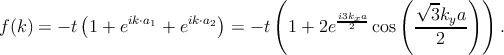 | (2.7) |
Solution of the secular equation det(H - EI) = 0 leads to the spectrum
 | (2.8) |
which is symmetric around zero energy. Here, t′ = 0 was assumed.
Electrical conduction is determined by the states around the Fermi energy and so it is useful to develop an approximate relation that describes the linear dispersion relation around E = 0. This can be done by replacing the expression for Eq. 2.7 with a Taylor expansion around one Dirac point k = K where the energy gap is zero. To simplify the derivation, we define a new wave vector relative to K which is called k′
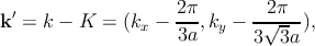 | (2.9) |
so we have
 | (2.10) |
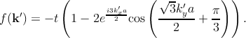
Now we consider the dispersion relation E(k′) which hols E(0) = 0. The Taylor expansion for new wave vector around (0, 0) gives
![[ ] [ ]
f ≈ k′ ∂f-- + k′ ∂f-- .
x ∂k′x k′=0 y ∂k ′y ′
k=0](diss45x.png) | (2.11) |
It is straightforward to evaluate the partial derivatives
![[ ∂f ] i3at [ ∂f ] 3at
---- = ----, ---- = - ----,
∂k ′x k′=0 2 ∂ky′ k′=0 2](diss46x.png) | (2.12) |
therefore
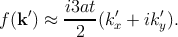 | (2.13) |
The corresponding energy dispersion relation (Eq. 2.8) shows a linear dependence
on the relation wavenumber |k′| = 
 | (2.14) |
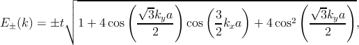
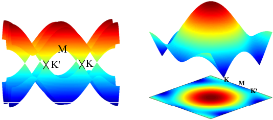
Figure 2.5 shows the electronic energy dispersion relations for graphene as a function of the two-dimensional wave-vector k in the hexagonal Brillouin zone. For finite values of t′, the electron-hole symmetry is broken and the π and π* bands become asymmetric.
The points K and K′, which specify six locations in momentum space, are called Dirac points, see Fig. 2.5. The conduction and valence bands meet at the Dirac points so graphene is a zero-gap material. The term ”massless Dirac fermions” is used to refer to linear dispersion relation E±(k) in Eq. 2.14. Electrons propagating through graphene behave as massless Dirac fermions because of the linear relation between their energy and their momentum [54].
 a),
and M = (2π∕3a, 0). The energy values at the K, M, and Γ points are 0, t,
and 3t, respectively.
a),
and M = (2π∕3a, 0). The energy values at the K, M, and Γ points are 0, t,
and 3t, respectively.Graphene has interesting properties which allow multiple functions of signal emitting, transmitting, modulating, and detection to be realized in one material. Graphene shows superior properties compared to silicon and III-V semiconductors in terms of its high thermal conductivity (~ 36 times higher than Si and ~ 100 times higher than GaAs), high optical damage threshold [55] (a few orders of magnitude higher than Si [56] and GaAs [57]), and high third-order optical nonlinearities (~ 3.3 × 10⁻¹⁶ coulomb) [58,59].
Due to the unique electronic structure in which conical-shaped conduction and valence bands meet at the Dirac point (Fig. 2.5), the optical conductance of pristine monolayer graphene is frequency-independent in a broad range of photon energies [60]. It is argued [61,62] that the high-frequency (dynamic) conductivity G for Dirac fermions [63] in graphene should be a universal constant equal to [64]
 | (2.15) |
where index ”l” refers to the real part, ω is the radian frequency, e is electron charge, and ℏ is reduced Planck’s constant. As a direct consequence of this universal optical conductance, the optical transmittance of pristine graphene is also frequency-independent and solely determined by the fine structure constant α = (1∕4πϵ0)(e2∕ℏc), where c is the speed of light, ϵ0 = 1∕μ0c2 is the permitivity of vacuum, and μ 0 is the permeability of vacuum. In the International System of Units (SI), c, ϵ0, and μ0 are exactly known constants. The optical transmittance of pristine graphene is defined as [65]
 | (2.16) |
When scaled to its atomic thickness, graphene actually shows strong broadband
absorption per unit mass of the material (πα = 2.3%), which is ~ 50 times higher
than GaAs of the same thickness [60,64,66]. The reflectance under normal light
incidence is relatively weak and written as R = 0.25π2α2T = 1.3 × 10⁻⁴, which is
much smaller than the transmittance [60]. The absorption of few-layer graphene
can be roughly estimated by scaling with the number of layers (T 1 -Nπα). In
principle, a low sheet resistance can be attained without sacrificing the
properties of transparency too much (i.e., tens of Ω∕□ for T > 90%). As
such, it is believed that few-layer graphene can potentially replace ITO
(indium tin oxide) as transparent conductors for applications in solar
cells [67–69] and touch screens [70–72] in cases when it is sufficiently
doped [65].
1 -Nπα). In
principle, a low sheet resistance can be attained without sacrificing the
properties of transparency too much (i.e., tens of Ω∕□ for T > 90%). As
such, it is believed that few-layer graphene can potentially replace ITO
(indium tin oxide) as transparent conductors for applications in solar
cells [67–69] and touch screens [70–72] in cases when it is sufficiently
doped [65].
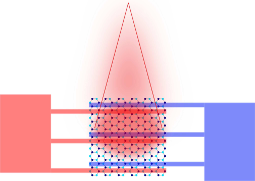
Based on the exciting optical properties of graphene, many graphene-based photonic and optoelectronic applications have been developed [70,73,74]. In this thesis we study the application of graphene-based structures as photodetectors (Fig. 2.6). Photodetectors measure the photon flux or optical power by converting the absorbed photon energy into electrical current [70]. They are used in various common devices in both science and technology [75], such as remote controls, televisions and DVD players. Modern light detectors are usually made using III-V semiconductors, such as gallium arsenide. When light strikes these materials, each absorbed photon creates an electron-hole pair (internal photoeffect). These pairs then separate and produce an electrical current. The spectral bandwidth is typically limited by the material’s absorption [75]. For example, photodetectors based on group IV and III-V semiconductors suffer from the ’long-wavelength limit’, as these become transparent when the incident energy is smaller than the bandgap [75]. A wide photon energy absorption range from the ultraviolet to terahertz could be covered by graphene-based photodetectors [60,76–78]. The response time is ruled by the carrier mobility [75] which is huge in graphene and thus ultrafast photodetectors are feasible [70].
The photoelectrical response of graphene has been widely investigated both experimentally and theoretically [48,79–82]. A photoresponse up to 40 GHz is reported for graphene photodetectors in [82]. The operating bandwidth is mainly limited by the time constant resulting from the device resistance and capacitance. Xia et al. reported an RC-limited bandwidth of about 640 GHz [82], which is comparable to traditional photodetectors [83]. However, the maximum possible operating bandwidth of photodetectors is typically restricted by their transit time [75].
The first application of graphene as a photodetector has been demonstrated in [84]. A detectable current has been reported that is attributed to the band bending at the metal/graphene interface [85]. Photocurrents have also been obtained at single/bilayer graphene interfaces [86] and graphene p-n junctions [87]. More recent studies concentrate on increasing the photoresponsivity of the graphene devices [88] and extending their operation range to longer wavelengths [89]. Recent photocurrent generation experiments in graphene show a strong photoresponse near metal/graphene interfaces, with an internal quantum efficiency of 15-30% despite its gapless nature [80,81,84]. Moreover, graphene photodetectors can potentially operate at speeds > 500GHz [82].
Although an external electric field can efficiently generate photocurrent with an electron-hole separation efficiency of over 30% [80], zero source-drain bias and dark current operations could be achieved by using the internal electric field formed near the metal electrode-graphene interfaces [48,82]. However, the small effective area of the internal electric field could decrease the detection efficiency [48,82], as most of the generated electron-hole pairs would be out of the electric field region, thus recombining, rather than being separated. The internal photocurrent efficiencies (15-30%; Refs [80,82]) and external responsivity (generated electric current for a given input optical power) of ~ 6.1 mA per Watt reported so far [48] are relatively low compared with current photodetectors [75]. This is mainly due to limited optical absorption when only one single layer graphene is used, short photocarrier lifetimes and small effective photodetection areas (~ 200 nm in [82]).