Previous: 2.1 Power Devices Overview Up: 2.1 Power Devices Overview Next: 2.1.2 Hybrid Integration and Intelligent Power Modules
Power semiconductor devices are used to control the energy transfer of electronic systems. Over the last two decades the technology of power semiconductors has made impressive progress [44,45,46,47]. The power function (switching or protection) is achieved through the combined use of low-voltage data and signal processing circuits [48,49,50] with power devices. The evolution naturally involves the integration of the whole or part of the low-voltage elements with the power devices [51,52,53,54] in order to improve performance and to reduce the chip (or system) size. The application of IC technologies on power semiconductor devices has offered efficient protection components, simple drive characteristics, and good control dynamics together with a direct interface to the monolithic integration with the signal processing circuitry on the same chip [55,56,57,58]. As a result, power electronic systems have greatly benefited from advances in power semiconductor technology. In consumer and industrial environments, designers make big efforts of improving the efficiency, to reduce the size and weight of components by combining the functions of several ICs and discrete power semiconductors. Thereby this the system costs can be lowered and the system design is simplified by reducing the number of components.
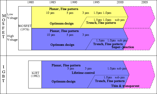
There are two distinct concepts for the development of power semiconductor devices. One concept involves discrete vertical power devices for medium- and high-power applications, and the other uses the lateral power devices for high-voltage (low-current) and smart power applications, and for monolithic integration with low-voltage circuitry. Discrete vertical power devices have evolved from bipolar devices (diodes, thyristors, GTOs, and BJTs) to power MOSFETs, IGBTs and MCTs [59,60]. Applications of discrete power devices are in the computer, telecommunications, and automotive industries for devices operating at below 300V and motor control, robotics, and power distribution for devices operating at above 300V. The most important step in the development of a new generation of power devices was the introduction of power MOSFETs [61,62]. The development of these new devices provided a direct link between integrated circuits and power devices. This evolution has led to power device development in terms of structure, design, size reduction, and manufacturing. The design rules reduction in discrete power MOSFETs has allowed a drastic reduction in the on-resistance drastically and in power dissipation. Another important breakthrough in the field of discrete devices has been the development of IGBTs combining the advantages of MOS transistors, such as low power drives by using MOS gate and fast switching, with the advantages of bipolar devices, such as low forward voltage drop by conductivity modulation in the drift region. Improvements in these new power devices, MOSFETs and IGBTs, are related to advances in standard MOS technology. These devices are produced in the same production facilities which were used for integrated circuits. The introduction of MOS technology in power electronics made it easy to integrate power devices into standard technology and integrated circuits have become compatible. For medium- and high-voltage applications IGBTs have been the dominated devices due to scaling of their voltage ratings and refinements to their gate structure achieved by using very large scale integration (VLSI) technology and trench gate regions. Figure 2.1 shows the development of power MOSFETs and IGBTs [63]. In the past ten years, MOSFET technology has been benefited from the drastic improvements achieved in the trench technology and in the characteristics of vertical super-junctions, while IGBT technology has shown improvements in performance due to lifetime control technology and structure enhancements.
Several types of MOS-gated thyristors have also been introduced, resulting in some promising improvements in the trade-off between on-state power loss, switching power loss, and the safe operating area. Improvements in power rectifiers have been achieved at low-voltage ratings using Schottky rectifier structures containing trenches and at high-voltage ratings using structures that combine junction and Schottky barrier contacts.
One of the most promising approaches in the field of power semiconductor devices
is the use of new materials such as silicon carbide (SiC) [64] and gallium nitride (GaN).
SiC Schottky rectifiers, power MESFETs, and power MOSFETs offer a significant
improvement in the trade-off between
![]() and the BV and in high-temperature
environments. The defect density and cost of the starting materials
determine the progress of commercialization of this technology.
and the BV and in high-temperature
environments. The defect density and cost of the starting materials
determine the progress of commercialization of this technology.
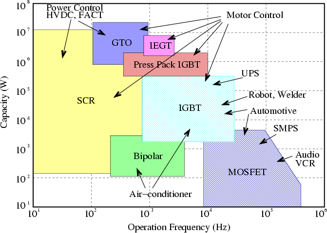
Figure 2.2 shows the application areas of discrete power semiconductors. As shown in the figure MOSFETs and IGBTs are used for high-frequency applications, and SCRs and GTOs are mainly used for high-power applications. For medium-power applications such as uninterruptible power supply (UPS), automotive, and robots IGBT or power MOSFET modules, which are constructed with series and parallel connection of power devices inside a plastic package, are used.
According to the area of application and the required performance, different modes of integration have been developed. A distinction must be made between monolithic and hybrid integration. The different developments have clearly shown that the medium- and high-power range can be implemented using hybrid integration which makes use of power parts and low-voltage parts in a package. For the low-power range (current (I) < 10A, voltage (V) < 600V) it can be implemented using monolithic integration of power semiconductor components and integrated circuits.
The evolution of lateral power device structures [65] has created a market for monolithic power integrated circuits that can incorporate sensors and protection functions.
Traditionally power semiconductor technology has always followed advances in VLSI technology. In addition to the improvements in photo-lithography and trench etching processes for power semiconductor structures, the capability for the integration of bipolar and CMOS structures with high-voltage devices has been greatly improved during the past fifteen years.
The basis for smart power technology is the integration of interface circuits, sensors, and protection circuitry with power devices. The interface function is made with CMOS circuits specially designed to operate in noisy and high temperature environments.
The high-voltage portion of the IC can either provide the entire power
control function as in the case of monolithic motor drives and lamp
ballast chips, or serve as the drive electronics for medium and
high-power devices in modules. The implementation of the
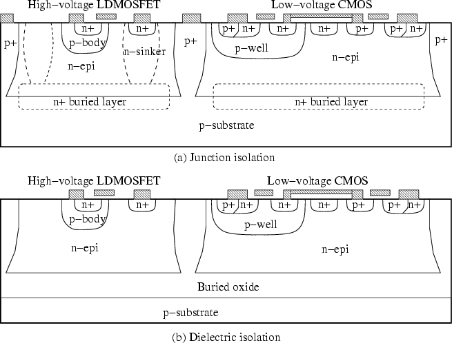
monolithic power IC technology was first done using junction
isolation as shown in Figure 2.3 (a). An important breakthrough in
the performance of high-voltage lateral MOSFETs which was required
for the applications was achieved by using the reduced surface field (RESURF)
principle, where the charge coupling between the drift region
and the ![]() -substrate is used to reduce the electric field
along the surface. With this approach, devices capable of
supporting more than 1200V have been made [66]. Some of the
drawbacks of junction isolation are the inability to integrate
bipolar structures due to mutual interaction and the high
leakage currents at elevated temperatures. To overcome
these problems, the RESURF concept was successfully extended
to dielectrically isolated structures, such as the
SOI-LDMOSFET (see Figure 2.3 (b)).
A systematic study of a variety of dielectrically isolated unipolar and bipolar
devices has been conducted for the purpose of integration.
Recently, significant improvements in the performance of lateral
power devices have been achieved by using
innovative lateral structures with charge coupled regions.
This section provides a review of the recent developments in power
semiconductor integration technology that are making a significant impact on
electronic systems.
-substrate is used to reduce the electric field
along the surface. With this approach, devices capable of
supporting more than 1200V have been made [66]. Some of the
drawbacks of junction isolation are the inability to integrate
bipolar structures due to mutual interaction and the high
leakage currents at elevated temperatures. To overcome
these problems, the RESURF concept was successfully extended
to dielectrically isolated structures, such as the
SOI-LDMOSFET (see Figure 2.3 (b)).
A systematic study of a variety of dielectrically isolated unipolar and bipolar
devices has been conducted for the purpose of integration.
Recently, significant improvements in the performance of lateral
power devices have been achieved by using
innovative lateral structures with charge coupled regions.
This section provides a review of the recent developments in power
semiconductor integration technology that are making a significant impact on
electronic systems.
Jong-Mun Park 2004-10-28