Previous: 4.1.1 Introduction Up: 4.1 Partial SOI-LDMOSFETs Next: 4.1.3 Simulation Results
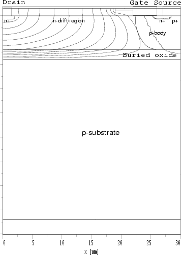
The schematic cross sections of the simulated devices are shown in Figure 4.1
to Figure 4.3. Generally, the BV of conventional SOI LDMOSFETs,
is limited by the buried oxide thickness, SOI thickness and the drift layer length.
Figure 4.1 shows a cross-sectional view of a conventional ![]() -channel SOI-LDMOSFET
designed for a BV of 300V with an SOI thickness
-channel SOI-LDMOSFET
designed for a BV of 300V with an SOI thickness
![]() of 7
of 7![]() m,
and with a buried oxide thickness
m,
and with a buried oxide thickness
![]() of 2
of 2![]() m.
The drift region of the device
is doped according to the RESURF principle to achieve a maximum
BV.
m.
The drift region of the device
is doped according to the RESURF principle to achieve a maximum
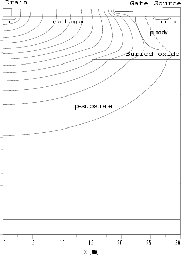
BV. ![]() -channel P-SOI LDMOSFETs with a silicon window under the drain
and under the source are shown in Figure 4.2 and Figure 4.3, respectively.
As shown in the figures, silicon is used as a window instead of some part of the
buried oxide layer. The major variable parameters are the
-channel P-SOI LDMOSFETs with a silicon window under the drain
and under the source are shown in Figure 4.2 and Figure 4.3, respectively.
As shown in the figures, silicon is used as a window instead of some part of the
buried oxide layer. The major variable parameters are the ![]() -substrate doping
concentration and the
-substrate doping
concentration and the ![]() -drift layer length. The
-drift layer length. The
![]() ,
,
![]() , and SOI layer
doping concentration of the P-SOI LDMOSFETs are the same as those of conventional
SOI LDMOSFETs shown in Figure 4.1.
, and SOI layer
doping concentration of the P-SOI LDMOSFETs are the same as those of conventional
SOI LDMOSFETs shown in Figure 4.1.
Jong-Mun Park 2004-10-28