Previous: 4.1.2 Device Structures Up: 4.1 Partial SOI-LDMOSFETs Next: 4.1.3.1 BV of P-SOI LDMOSFETs
Optimal trade-off between BV and
![]() has been the main issue of these devices.
P-SOI structures help to increase the BV while maintaining
has been the main issue of these devices.
P-SOI structures help to increase the BV while maintaining
![]() ,
and reduce the self-heating problems by using high thermally
conductive silicon as a window.
,
and reduce the self-heating problems by using high thermally
conductive silicon as a window.
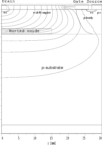
The potential distribution of the conventional SOI-LDMOSFET and the P-SOI LDMOSFETs at breakdown are shown in Figures 4.1 - 4.3. In conventional SOI-LDMOSFETs, a large voltage drops in the buried oxide, and it prevents potential lines from spreading into the substrate ( Figure 4.1). Almost all the voltage drops in the buried oxide layer. The maximum electric field in the buried oxide is determined by the electric field at the interface between the silicon and the buried oxide. To obtain a higher BV with thick film SOI-LDMOSFETs, the buried oxide thickness or the SOI layer thickness must be increased. As these parameters are increased to improve the BV, however, the thermal characteristics of the devices will degrade.
In the case of the P-SOI LDMOSFET, however, potential lines spread into the substrate. As shown in Figure 4.2, the potential distribution of a P-SOI LDMOSFET with a silicon window under the drain is similar to that of standard junction isolation devices.
Part of the voltage will drop in the depletion layer in the substrate region. However, the buried oxide layer does not affect the BV in this structure. The buried oxide is used only for the isolation of power devices and low-voltage circuitry. In P-SOI LDMOSFETs with a silicon window under the source ( Figure 4.3) the potential distribution in the buried oxide layer is similar to that of conventional SOI-LDMOSFETs, so the buried oxide layer helps to increase the BV together with the depletion region in the substrate. In addition, the temperature rise due to self-heating is reduced by the silicon window in P-SOI LDMOSFETs. Two-dimensional numerical simulations with MINIMOS-NT have been performed to investigate the influence of the window on the BV and the self-heating effects.