
Previous: 4.4.1 Introduction Up: 4.4 SJ SOI-LDMOSFETs with Reduced Drift Length Next: 4.4.3 Simulation Results
Figure 4.31 shows the schematic structure of the proposed SJ SOI-LDMOSFET which has a trench oxide in the drift region.
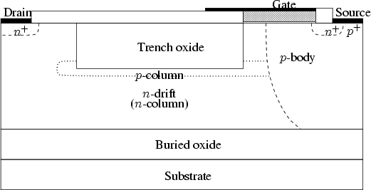 |
This structure can be made
by introducing buried ![]() -columns in the drift region and by an additional
trench process.
Generally, the maximum BV of conventional SOI-LDMOSFETs
is limited by the thickness of the buried oxide.
The optimum drift
length must be ensured to get the best trade-off between
-columns in the drift region and by an additional
trench process.
Generally, the maximum BV of conventional SOI-LDMOSFETs
is limited by the thickness of the buried oxide.
The optimum drift
length must be ensured to get the best trade-off between
![]() and the BV.
With the structure proposed it is possible to reduce the drift length
drastically without degrading the maximum BV by increasing the surface
path of the drift layer.
This buried
and the BV.
With the structure proposed it is possible to reduce the drift length
drastically without degrading the maximum BV by increasing the surface
path of the drift layer.
This buried ![]() -column can be connected to the
-column can be connected to the ![]() -body directly or indirectly.
The optimum
-body directly or indirectly.
The optimum ![]() -column doping concentration is determined by the width
of the
-column doping concentration is determined by the width
of the ![]() -column and the net charge of the
-column and the net charge of the ![]() -column.
-column.
Our device is designed to achieve a BV of 300V with an SOI thickness
![]() of
7.0
of
7.0![]() m and with a buried oxide thickness
m and with a buried oxide thickness
![]() of 2.0
of 2.0![]() m. With these
structure parameters the maximum BV of conventional SOI-LDMOSFETs is 300V at the
minimum allowable drift length of 20.0
m. With these
structure parameters the maximum BV of conventional SOI-LDMOSFETs is 300V at the
minimum allowable drift length of 20.0![]() m.
m.
The main focus of the study
is to optimize the device parameters of the proposed structure shown in Figure 4.31.
The trench oxide depth affects the BV and it must be designed to ensure a long enough
surface path of the device.
It is important to minimize the ![]() -column width, because it shrinks the
conduction area of the device. The
-column width, because it shrinks the
conduction area of the device. The ![]() - and
- and ![]() -column doping concentrations are a
function of the column width. The
-column doping concentrations are a
function of the column width. The ![]() -column doping must be increased to lower
the on-resistance of the SJ devices.
-column doping must be increased to lower
the on-resistance of the SJ devices.
Simulations are performed to find optimum device parameters with a
trench oxide depth from 2.0 to 3.0![]() m and a
m and a ![]() -column width from 0.3 to
1.3
-column width from 0.3 to
1.3![]() m.
With an
m.
With an ![]() -column width
-column width
![]() of 4.0
of 4.0![]() m, a
m, a ![]() -column width
-column width
![]() of
0.3
of
0.3![]() m and a drift length
m and a drift length
![]() of 13.0
of 13.0![]() m the doping concentration of
the
m the doping concentration of
the ![]() -column can be raised up to 6.0
-column can be raised up to 6.0 ![]()
![]()
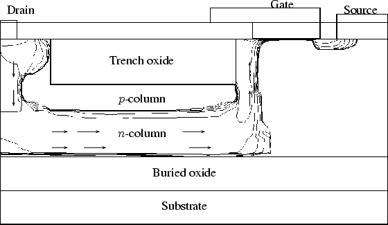
![]() . As shown in
Figure 4.32, the current of the proposed structure flows
through the
. As shown in
Figure 4.32, the current of the proposed structure flows
through the ![]() -column. The figure shows clearly that only the
-column. The figure shows clearly that only the
![]() -column contributes to the current conduction.
-column contributes to the current conduction.
 |