
Previous: 4.4.2 Device Structures and Operations Up: 4.4 SJ SOI-LDMOSFETs with Reduced Drift Length Next: 4.5 Shorted-Anode LIGBT on SOI with Trench Oxide
![]() and the BV of high-voltage SOI-LDMOSFETs strongly depend on the doping and
the length of the drift layer. The drift doping of conventional
SOI-LDMOSFETs is restricted by the RESURF effect.
To increase the BV the drift length must be increased and the doping decreased.
This results in an increase in the on-resistance.
With the SJ structure it is possible to increase the doping concentration
of the drift layer drastically, and
and the BV of high-voltage SOI-LDMOSFETs strongly depend on the doping and
the length of the drift layer. The drift doping of conventional
SOI-LDMOSFETs is restricted by the RESURF effect.
To increase the BV the drift length must be increased and the doping decreased.
This results in an increase in the on-resistance.
With the SJ structure it is possible to increase the doping concentration
of the drift layer drastically, and
![]() can be reduced effectively.
can be reduced effectively.
The on-resistance of SJ devices has a linear voltage dependence instead
of the square-law dependence of standard power MOSFETs [75,159].
The BV of the SJ depends on the critical electric field
![]() of the device and the length
of the
of the device and the length
of the ![]() - and
- and ![]() -columns. With the SJ concept
the
-columns. With the SJ concept
the ![]() -column charge
-column charge
![]() , the
, the ![]() -column
charge
-column
charge
![]() , and the charge
, and the charge
![]() of the
of the ![]() -body depletion region should be balanced
in this structure.
To reduce the column length of the SJ SOI-LDMOSFET a trench
oxide is proposed in this study.
-body depletion region should be balanced
in this structure.
To reduce the column length of the SJ SOI-LDMOSFET a trench
oxide is proposed in this study.
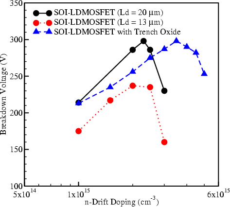
Figure 4.33 shows a comparison of the BV of conventional
SOI-LDMOSFETs which have an ![]() -drift length
-drift length
![]()
![]() 20.0
20.0![]() m and 13.0
m and 13.0![]() m,
respectively, and the SJ SOI-LDMOSFET with a trench oxide and
m,
respectively, and the SJ SOI-LDMOSFET with a trench oxide and
![]()
![]() 13.0
13.0![]() m. As shown in the figure the BV of the conventional devices
strongly depends on the drift length. The conventional SOI-LDMOSFET with
m. As shown in the figure the BV of the conventional devices
strongly depends on the drift length. The conventional SOI-LDMOSFET with
![]()
![]() 7.0
7.0![]() m and
m and
![]()
![]() 2.0
2.0![]() m has a BV of 300V
(the solid line) at
m has a BV of 300V
(the solid line) at
![]()
![]() 20.0
20.0![]() m and
m and
![]()
![]() 2.3
2.3 ![]()
![]()
![]() . If the
. If the ![]() -drift length is reduced to 13.0
-drift length is reduced to 13.0![]() m
in this structure, a BV of 245V (the dotted line) is obtained at
m
in this structure, a BV of 245V (the dotted line) is obtained at
![]()
![]() 3.5
3.5 ![]()
![]()
![]() . The dashed line in the figure shows the
BV of the SJ SOI-LDMOSFET with a trench oxide.
. The dashed line in the figure shows the
BV of the SJ SOI-LDMOSFET with a trench oxide.
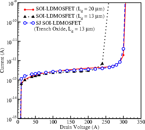 |
Because of the increased surface
path of the device, the BV increases with the trench oxide in the drift region.
A BV of 300V is obtained with
![]()
![]() 13.0
13.0![]() m in this structure.
Note that this is the same BV as that of the conventional SOI-LDMOSFET
with
m in this structure.
Note that this is the same BV as that of the conventional SOI-LDMOSFET
with
![]()
![]() 20.0
20.0![]() m.
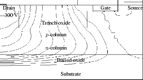
Figure 4.34 shows the potential distribution of the RESURF SJ SOI-LDMOSFET
which has a trench oxide and
m.
Figure 4.34 shows the potential distribution of the RESURF SJ SOI-LDMOSFET
which has a trench oxide and
![]()
![]() 13.0
13.0![]() m.
Because of the increased surface path to the vertical direction in the drift region,
we can see potential lines at the side wall of the trench oxide.
These potential lines help to increase the BV to the
maximum value of conventional SOI-LDMOSFETs with
m.
Because of the increased surface path to the vertical direction in the drift region,
we can see potential lines at the side wall of the trench oxide.
These potential lines help to increase the BV to the
maximum value of conventional SOI-LDMOSFETs with
![]()
![]() 20.0
20.0![]() m.
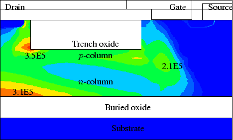
Figure 4.35 shows the electric field distribution of the suggested device at
m.
Figure 4.35 shows the electric field distribution of the suggested device at
![]() = 300V. Note that a higher electric field can be observed at the trench oxide edges.
From this figure we can see clearly several peaks of the electric field.
The SJ SOI-LDMOSFET with a trench oxide has an additional peak in the
middle of the SOI layer below the gate.
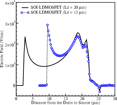
Figure 4.36 shows a comparison of the electric field at the top surface
between conventional SOI-LDMOSFETs with
= 300V. Note that a higher electric field can be observed at the trench oxide edges.
From this figure we can see clearly several peaks of the electric field.
The SJ SOI-LDMOSFET with a trench oxide has an additional peak in the
middle of the SOI layer below the gate.
Figure 4.36 shows a comparison of the electric field at the top surface
between conventional SOI-LDMOSFETs with
![]()
![]() 20.0
20.0![]() m and 13.0
m and 13.0![]() m.
Conventional SOI-LDMOSFETs have the peak electric field at the drain,
the field plate, and the gate edge near the top surface of the silicon.
m.
Conventional SOI-LDMOSFETs have the peak electric field at the drain,
the field plate, and the gate edge near the top surface of the silicon.
 |
 |
 |
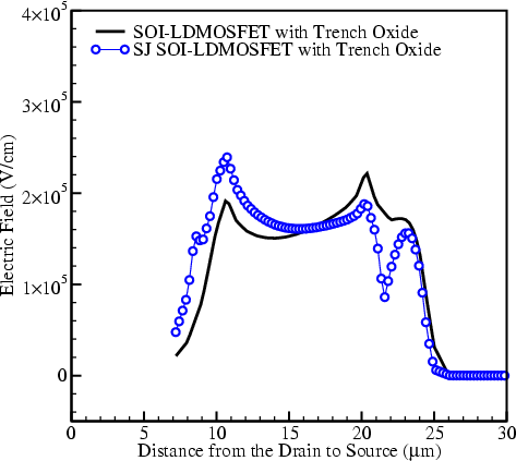 |
Figure 4.37 shows a comparison of the electric field
at the bottom of the trench oxide between the SOI-LDMOSFET and the SJ
SOI-LDMOSFET.
![]() of both structures is 13.0
of both structures is 13.0![]() m.
At the
m.
At the ![]() -drift and
-drift and ![]() -body junction both devices show similar trends
as those of the conventional device, but the abrupt peak can be seen at the
trench oxide edge.
Generally, in the middle of the device (along the lateral
direction of the device) the conventional SOI-LDMOSFET has a broad range of higher
electric field near the
-body junction both devices show similar trends
as those of the conventional device, but the abrupt peak can be seen at the
trench oxide edge.
Generally, in the middle of the device (along the lateral
direction of the device) the conventional SOI-LDMOSFET has a broad range of higher
electric field near the ![]() -drift and
-drift and ![]() -body junction, and no abrupt peak can
be found. For the SJ SOI-LDMOSFET with a trench oxide of
-body junction, and no abrupt peak can
be found. For the SJ SOI-LDMOSFET with a trench oxide of
![]()
![]() 13.0
13.0![]() m and
m and
![]()
![]() 6.0
6.0 ![]()
![]()
![]() ,
the optimum electric field distribution is obtained with
,
the optimum electric field distribution is obtained with
![]() of
1.5
of
1.5 ![]()
![]()
![]() (with
(with
![]()
![]() 0.8
0.8![]() m).
m).
The solid line of Figure 4.38 shows the BV versus ![]() -drift doping
of the conventional SOI-LDMOSFET with an optimum
-drift doping
of the conventional SOI-LDMOSFET with an optimum
![]()
![]() 20.0
20.0![]() m.
To achieve the best trade-off between
m.
To achieve the best trade-off between
![]() and the BV, a higher drift
doping with optimum
and the BV, a higher drift
doping with optimum
![]() is essential.
From the figure we can see the optimum
is essential.
From the figure we can see the optimum ![]() -drift doping is 2.3
-drift doping is 2.3 ![]()
![]()
![]() .
If the
.
If the ![]() -drift doping is reduced
below the optimum value, the maximum electric field is moved towards the drain edge.
If it exceeds the optimum value, a high electric field is moved towards
the gate edge. Both cases cause a lower BV.
-drift doping is reduced
below the optimum value, the maximum electric field is moved towards the drain edge.
If it exceeds the optimum value, a high electric field is moved towards
the gate edge. Both cases cause a lower BV.
![]() can be lowered by
reducing
can be lowered by
reducing
![]() . This shrinks the surface path of the depletion region at breakdown.
. This shrinks the surface path of the depletion region at breakdown.
The dotted line of the figure shows the BV of a conventional SOI-LDMOSFET with
![]()
![]() 13.0
13.0![]() m, where a maximum BV of 245V is obtained at
m, where a maximum BV of 245V is obtained at
![]()
![]() 2.0
2.0 ![]()
![]()
![]() . With the trench oxide in the drift region
it is possible to increase the surface path of the depletion region and
. With the trench oxide in the drift region
it is possible to increase the surface path of the depletion region and
![]() can be
reduced drastically without degrading the BV. The dashed line shows the BV of
the SOI-LDMOSFET which has a trench oxide in the drift region and a maximum BV of 300V
is obtained at
can be
reduced drastically without degrading the BV. The dashed line shows the BV of
the SOI-LDMOSFET which has a trench oxide in the drift region and a maximum BV of 300V
is obtained at
![]()
![]() 13.0
13.0![]() m. Because the reduced
m. Because the reduced ![]() -drift area by the trench oxide
affects the charge balance condition, the optimum doping
-drift area by the trench oxide
affects the charge balance condition, the optimum doping
![]() is slightly increased
compared to the conventional device.
is slightly increased
compared to the conventional device.
 |
 |
 |
The reduced conduction area by the trench oxide increases
![]() .
To solve this problem we propose the SJ SOI-LDMOSFET by introducing the buried
.
To solve this problem we propose the SJ SOI-LDMOSFET by introducing the buried
![]() -column in the
-column in the ![]() -drift region together with a trench oxide. With this structure
-drift region together with a trench oxide. With this structure
![]() can be lowered effectively.
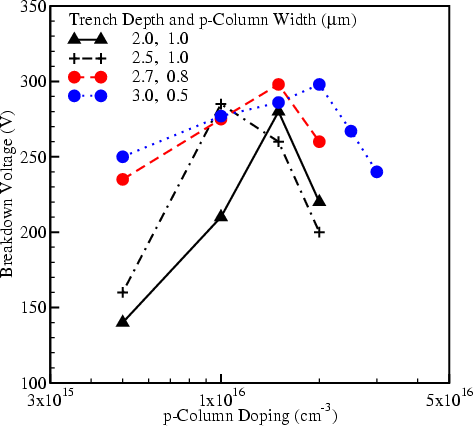
Figure 4.39 shows
the BV versus
can be lowered effectively.
Figure 4.39 shows
the BV versus ![]() -column doping of the proposed devices with various trench depths.
-column doping of the proposed devices with various trench depths.
![]() and
and
![]() are fixed to 13.0
are fixed to 13.0![]() m and 6.0
m and 6.0 ![]()
![]()
![]() , respectively.
, respectively.
The trench depth determines the length of the surface path of the device. If it
is below 2.5![]() m (solid and dot-dashed lines) the BV is lower than
that of conventional devices. With the trench depth over 2.7
m (solid and dot-dashed lines) the BV is lower than
that of conventional devices. With the trench depth over 2.7![]() m the same
BV is reached as the maximum value of conventional SOI-LDMOSFETs.
m the same
BV is reached as the maximum value of conventional SOI-LDMOSFETs.
To obtain a maximum BV,
![]() ,
,
![]() , and
, and
![]() in the SJ
SOI-LDMOSFET should be balanced for complete depletion of the drift region
at breakdown. If the
in the SJ
SOI-LDMOSFET should be balanced for complete depletion of the drift region
at breakdown. If the
![]() -column width is larger, the doping of this layer should be reduced to fulfill the
charge balance. It is also important to minimize the
-column width is larger, the doping of this layer should be reduced to fulfill the
charge balance. It is also important to minimize the ![]() -column width to increase the
area of current path at the drift region.
-column width to increase the
area of current path at the drift region.
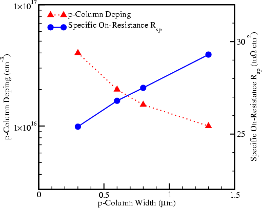
Figure 4.40 shows the ![]() -column doping and
-column doping and
![]() versus the
versus the ![]() -column width of
the proposed SJ SOI-LDMOSFET which has a trench oxide. The
-column width of
the proposed SJ SOI-LDMOSFET which has a trench oxide. The ![]() -column doping
concentration at each point
in the figure is optimized to have a maximum BV of 300V.
Other device parameters such as the trench oxide depth, the drift length
-column doping
concentration at each point
in the figure is optimized to have a maximum BV of 300V.
Other device parameters such as the trench oxide depth, the drift length
![]() ,
and the
,
and the ![]() -column doping
-column doping
![]() are 2.7
are 2.7![]() m, 13.0
m, 13.0![]() m,
and 6.0
m,
and 6.0 ![]()
![]()
![]() , respectively.
The doping of the
, respectively.
The doping of the ![]() -column is reduced with the increased
-column is reduced with the increased ![]() -column width.
-column width.
The dotted line of Figure 4.40 clearly denotes this dependence.
With
![]()
![]() 0.3 and 1.3
0.3 and 1.3![]() m, the
optimum
m, the
optimum
![]() is 4.0 and 1.0
is 4.0 and 1.0 ![]()
![]()
![]() , respectively.
, respectively.
![]()
![]()
![]()
![]()
![]() of both cases remains approximately constant.
The solid line shows the relationship between
of both cases remains approximately constant.
The solid line shows the relationship between
![]() and
and
![]() .
With reduced
.
With reduced ![]() -column width
-column width
![]() is improved by the increased conduction area.
With a lower value for
is improved by the increased conduction area.
With a lower value for
![]() of 0.3
of 0.3![]() m it is possible to achieve a minimum
m it is possible to achieve a minimum
![]() of
25.4m
of
25.4m![]()
![]() . If
. If
![]() is increased to 1.3
is increased to 1.3![]() m,
m,
![]() is increased to 29.3m
is increased to 29.3m![]()
![]() .
.
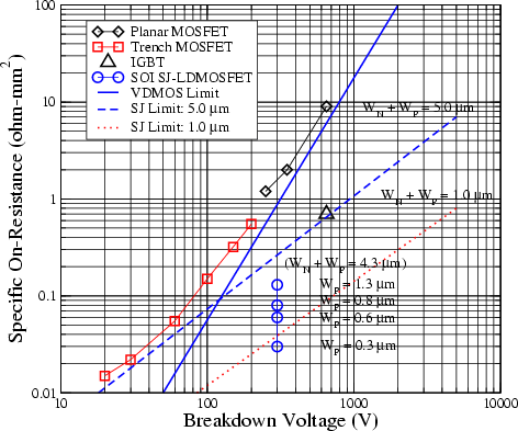 |
Figure 4.41 shows the
![]() versus BV comparison
with conventional MOSFETs, theoretical Si limit, and proposed SJ SOI-LDMOSFETs.
AS shown in the figure lower values of
versus BV comparison
with conventional MOSFETs, theoretical Si limit, and proposed SJ SOI-LDMOSFETs.
AS shown in the figure lower values of
![]() can be obtained with the proposed
SJ SOI-LDMOSFETs which have a trench oxide in the drift region.
This is mainly because of the reduced drift length by the trench oxide.
can be obtained with the proposed
SJ SOI-LDMOSFETs which have a trench oxide in the drift region.
This is mainly because of the reduced drift length by the trench oxide.
|
Conventional SOI-LDMOSFET |
Proposed SJ SOI-LDMOSFET |
|
|
|
2.3 |
6.0 |
|
|
20.0 |
13.0 |
|
|
33.4m |
25.4m |
| BV | 300V | 300V |
Table 4.4 shows a DC performance comparison of the simulation results between
the conventional SOI-LDMOSFET and the proposed SJ SOI-LDMOSFET which has a
trench oxide in the drift region.
For the proposed device with an n-column doping
![]() of 6.0
of 6.0 ![]()
![]()
![]() and a drift length
and a drift length
![]() of 13.0
of 13.0![]() m, a maximum BV of 300V is obtained at
the p-column doping
m, a maximum BV of 300V is obtained at
the p-column doping
![]()
![]() 4.0
4.0 ![]()
![]()
![]() and the p-column width
and the p-column width
![]()
![]() 0.3
0.3![]() m. These results demonstrate that the drift length can be reduced
with a trench oxide in the drift region.
The on-state characteristics depend on the
m. These results demonstrate that the drift length can be reduced
with a trench oxide in the drift region.
The on-state characteristics depend on the ![]() -column width and the drift doping.
-column width and the drift doping.
![]() of the proposed device is 25.4m
of the proposed device is 25.4m![]()
![]() . It is about 76% of the
corresponding
. It is about 76% of the
corresponding
![]() of the conventional 300V SOI-LDMOSFET.
Even the width of the drift region is reduced by the
of the conventional 300V SOI-LDMOSFET.
Even the width of the drift region is reduced by the ![]() -column and
-column and
![]() is lower than that of the conventional device by the reduced
is lower than that of the conventional device by the reduced
![]() and
the increased
and
the increased
![]() of the proposed device.
of the proposed device.
Jong-Mun Park 2004-10-28