Near field scanning over a PCB is a state of the art method to investigate the EMC
performance experimentally [81], [82]. Usually the
magnetic field vector components  ,
,  and
and
 are scanned versus frequency as depicted in
Figure 5.10. Phase information can either be obtained with a double probe
time domain scanner [83], [84], or by the method of
[85], which obtains the phase from two magnitude scans with different
scan heights above the PCB.
are scanned versus frequency as depicted in
Figure 5.10. Phase information can either be obtained with a double probe
time domain scanner [83], [84], or by the method of
[85], which obtains the phase from two magnitude scans with different
scan heights above the PCB.
Figure 5.10:
Scanning the magnetic field above the PCB with a magnetic field probe.
|
![\includegraphics[width=12cm,viewport=92 520 510 760,clip]{{pics/PCB_Scan.eps}}](img386.png) |
Increased field value areas on the PCB are observed as potential electromagnetic
emission sources. However, there is actually no direct relation from the scanned field
values to the coupling of the PCB to a cavity field. The coupling of an IC to the cavity
field inside a  TEM cell is tested with the standardized IC EMC compliant measurement
of [54]. Therefore, investigations have been carried out to predict the results
of these IC TEM measurements with scanned field data and with simulations.
[81] utilizes empirical formulations for a first order prediction of
TEM cell IC measurements from near field measurement data.
[6] and [52] modeled the coupling from an IC to a
TEM cell with coupling capacitors. These models had some inaccuracies especially for
frequencies above 300MHz and did not reveal any relationship to the near field above the
IC. Only three-dimensional full wave simulations or the mulipole method of
[31] enable an accurate prediction of the PCB or IC cavity coupling from
near field data. However, these methods do not preserve the initial near field
localization of the critical sources on the PCB.
TEM cell is tested with the standardized IC EMC compliant measurement
of [54]. Therefore, investigations have been carried out to predict the results
of these IC TEM measurements with scanned field data and with simulations.
[81] utilizes empirical formulations for a first order prediction of
TEM cell IC measurements from near field measurement data.
[6] and [52] modeled the coupling from an IC to a
TEM cell with coupling capacitors. These models had some inaccuracies especially for
frequencies above 300MHz and did not reveal any relationship to the near field above the
IC. Only three-dimensional full wave simulations or the mulipole method of
[31] enable an accurate prediction of the PCB or IC cavity coupling from
near field data. However, these methods do not preserve the initial near field
localization of the critical sources on the PCB.
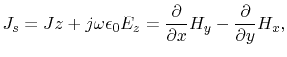
It has previously been described that only the vertical current segments couple to the
cavity. This enables a direct relation to be expressed from the scanned near field to the
common mode coupling. The third Maxwell equation in air
 |
(5.13) |
relates the magnetic field density  to the electric field density,
  and
the current density
and
the current density  . The dielectric constant in air is
 .
Equation (5.13) is utilized to express the vertical current density
.
Equation (5.13) is utilized to express the vertical current density
 |
(5.14) |
which excites the cavity field. This current density can be introduced into a cavity
model with the weighting factor
 |
(5.15) |
where  denotes the height of the scanning plane above the parallel ground plane.
When a scan would be carried out directly on the trace, without any distance of the scan
plane (theoretically), the current
denotes the height of the scanning plane above the parallel ground plane.
When a scan would be carried out directly on the trace, without any distance of the scan
plane (theoretically), the current  would become the trace current and the
coupling weighting factor would become
would become the trace current and the
coupling weighting factor would become  . Equation (5.14)
reveals that not the field density values, but their derivatives are significant for the
common mode coupling to the cavity. Therefore, a scan plot
of 5.14 will provide much more precision for coupling source
identification. Figure 5.11 depicts both, and
. Equation (5.14)
reveals that not the field density values, but their derivatives are significant for the
common mode coupling to the cavity. Therefore, a scan plot
of 5.14 will provide much more precision for coupling source
identification. Figure 5.11 depicts both, and
 , along a short trace in y-direction. The vertical segments that couple
to the cavity can clearly be localized from
. is
nearly constant along the whole horizontal trace segment which does not couple to the
cavity.
For maximum source localization accuracy, the scan has to be performed as close as
possible along the PCB or IC surfaces and the scan heights above the PCB ground plane
must be taken into account using (5.15) for the
classification of the source coupling potentials.
, along a short trace in y-direction. The vertical segments that couple
to the cavity can clearly be localized from
. is
nearly constant along the whole horizontal trace segment which does not couple to the
cavity.
For maximum source localization accuracy, the scan has to be performed as close as
possible along the PCB or IC surfaces and the scan heights above the PCB ground plane
must be taken into account using (5.15) for the
classification of the source coupling potentials.
![\includegraphics[width=10cm,viewport=120 580 510
760,clip]{{pics/Scan_PCB_trace.eps}}](img391.png)
Figure 5.11:
and
along the y direction.
enables an accurate identification of the coupling
current segments, while is high along the whole trace length.
The following subsections describe some application opportunities for
(5.14) and (5.15) beyond
source identification.
Subsections
C. Poschalko: The Simulation of Emission from Printed Circuit Boards under a Metallic Cover