|
|
|
|
Dissertation Christian Poschalko | Previous: 4.4 FEM solution for the two-dimensional Helmholtz equation Up: Contents Next: 5.1 Calculation of with mode decomposition |
|
|
|
|
Dissertation Christian Poschalko | Previous: 4.4 FEM solution for the two-dimensional Helmholtz equation Up: Contents Next: 5.1 Calculation of with mode decomposition |
Efficient power integrity analysis with cavity models for rectangular power planes
obtained from (4.13) and (4.14) have been
presented by [42] and [43]. While power-ground planes are excited
by currents, which are galvanically supplied to the planes, an enclosure is excited by
common mode coupling from a PCB trace to the cavity between the ground plane and the
cover. Since the models (4.13) and (4.14)
can only be excited by currents supplied to the planes, the common mode coupling of a
trace also has to be introduced into these models by current sources, connected to the
upper and lower plane.
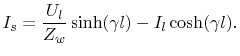
According to conditions (4.4)
and (4.5) only the TMzm (magnetic field transversal in the z
direction) mode m=0 is considered in the cavity model and the electric field has thus
only a z-component. This is also sufficient in case of a trace within the cavity, because
higher order parallel plate modes, excited by the horizontal trace current, decay rapidly
and cannot reach the surrounding edges. Therefore, any horizontal current can be
neglected and the vertical trace currents at the source ![]() and load
and load ![]() positions
(Figure 5.1) couple to the cavity. Excitations are introduced
into the cavity model (4.13) by vertical currents on ports
between the upper and lower plane.
positions
(Figure 5.1) couple to the cavity. Excitations are introduced
into the cavity model (4.13) by vertical currents on ports
between the upper and lower plane.
![\includegraphics[width=13cm,viewport=110 575 490
760,clip]{{pics/Trace_Introduction.eps}}](img328.png) |
The port excitation currents in Figure 5.1(b) are the trace
currents at the source (s) and the load (l) in Figure 5.1 (a)
multiplied by the constant factor
![]() . This mode conversion factor accounts for
the coupling from the trace to the common mode cavity field. Port m in
Figure 5.1 has been introduced for the voltage measurement
between the planes. With (4.17), the voltage on the test port
. This mode conversion factor accounts for
the coupling from the trace to the common mode cavity field. Port m in
Figure 5.1 has been introduced for the voltage measurement
between the planes. With (4.17), the voltage on the test port
![]() can be expressed by
can be expressed by
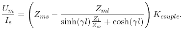
Since (5.6) does not consider the back coupling from the cavity field to the trace, it is valid in case of emission simulation, where the trace currents are determined by the trace geometry above the ground plane, the source, and the load. The dielectric layers in printed circuit boards are usually thin, compared to the distance from the ground plane to a parallel metallic enclosure cover. Therefore, the influence of the metallic cover plane on the characteristic impedance of the traces is negligible and the currents on the traces can be simulated with this characteristic impedance, the driver, and the load models. Characteristic impedances with and without the metallic cover plane can be compared with numerical simulation.
![\includegraphics[width=7cm,viewport=155 645 375 750,clip]{{pics/EffectivLength.eps}}](img336.png)