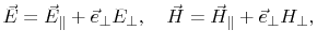
8.2 Rule 2: Trace placement parallel and close to metallic enclosure walls reduces
EMI, trace placement orthogonal and close to enclosure walls increases EMI
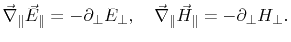
Figure 8.2(b) shows a radiated power reduction of 20dB over the whole
frequency range from 100MHz to 4GHz when the trace placement is changed from that of
Trace A to that of Trace B, as depicted in Figure 8.2(a). It is recommended to
place critical traces parallel and close to the metallic enclosure walls. This must
already be considered, when placing the driver and receiver ICs on the PCB.
![\includegraphics[height=5 cm]{pics/MotorSG.eps}](img592.png)
| (a) Placement of Trace A and Trace B. |
![\includegraphics[height=9 cm,viewport=75 460 540
780,clip]{pics/Design_rule2.eps}](img593.png)
| (b) Overall radiated power from the enclosure slot. |
|
Figure 8.2:
The trace width is 0.2mm, the trace height above the ground plane is 0.65mm. A
10mV voltage source with an impedance equal to the characteristic impedance of the trace
 drives the trace which is terminated with a 10pF capacitance.
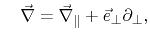
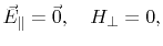
Trace B in Figure 8.2(a) is closer to the back wall than Trace A. Therefore,
it cannot be determined which part of the emission reduction in Figure 8.2(b)
is obtained from the closer placement and which part from the parallel placement of Trace
B to the enclosure wall. Therefore, Figure 8.3 depicts the
comparison with a Trace B parallel to the enclosure wall at the maximum distance of Trace
A from that wall. The result of the comparison in Figure 8.3(b) shows that
10dB of the 20dB in Figure 8.2(b) reduction can be assigned to the parallel
placement and 10dB to the closer placement.
![\includegraphics[height=5 cm]{pics/MotorSG.eps}](img594.png)
| (a) Placement of Trace A and Trace B. |
![\includegraphics[height=9 cm,viewport=75 460 540
780,clip]{pics/Design_rule2.eps}](img595.png)
| (b) Overall radiated power from the enclosure slot. |
|
Figure 8.3:
The trace width is 0.2mm, the trace height above the ground plane is 0.65mm. A
10mV voltage source with an impedance equal to the characteristic impedance of the trace
drives the trace which is terminated with a 10pF capacitance.
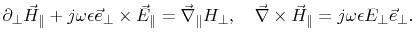
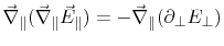
The same emission reduction of 20dB is also observed in Figure 8.4,
when the Trace B is arranged closer and parallel to a side wall of the enclosure.
![\includegraphics[height=5 cm]{pics/MotorSG.eps}](img596.png)
| (a) Placement of Trace A and Trace B. |
![\includegraphics[height=9 cm,viewport=75 460 540
780,clip]{pics/Design_rule2.eps}](img597.png)
| (b) Overall radiated power from the enclosure slot. |
|
Figure 8.4:
The trace width is 0.2mm, the trace height above the ground plane is 0.65mm. A
10mV voltage source with an impedance equal to the characteristic impedance of the trace
drives the trace which is terminated with a 10pF capacitance.
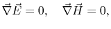
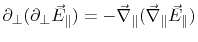
A comparison with a Trace B parallel to the enclosure wall at the maximum distance of
Trace A from that wall in Figure 8.5 shows a similar result as for
the back wall. Nearly 10dB emission reduction is achieved with a closer placement of the
trace to the enclosure wall and 10dB reduction results from the orientation of the trace
parallel to the wall.
![\includegraphics[height=5 cm]{pics/MotorSG.eps}](img598.png)
| (a) Placement of Trace A and Trace B. |
![\includegraphics[height=9 cm,viewport=75 460 540
780,clip]{pics/Design_rule2.eps}](img599.png)
| (b) Overall radiated power from the enclosure slot. |
|
Figure 8.5:
The trace width is 0.2mm, the trace height above the ground plane is 0.65mm. A
10mV voltage source with an impedance equal to the characteristic impedance of the trace
drives the trace which is terminated with a 10pF capacitance.
The design rule is generalized to fairly arbitrary shaped, and even electrically large
metallic enclosures as follows. The field inside a metallic enclosure can generally be
described by an eigenfunction superposition. Since the eigenfunctions can be obtained
from a homogenous solution of the Maxwell equations, the following investigation of the
field close to a metallic enclosure wall is carried out from the homogenous Maxwell
equations. A smooth metallic enclosure surface can be approximated locally by the
tangential plane. The fields close to a metallic plane are expressed in a coordinate
system with one coordinate direction normal (index ^) to the plane and two
coordinate directions parallel (index ||) to the plane. The electric field, the
magnetic field, and the vector operator  are expressed within this
coordinate system. With
are expressed within this
coordinate system. With
 and and
 |
(8.1) |
the Maxwell curl equations for the electric field become

|
(8.2) |
and the Maxwell curl equations for the magnetic field become
 |
(8.3) |
From the Maxwell divergence equations
|
(8.4) |
follows
|
(8.5) |
With consideration of the PEC boundary at the metallic plane
 |
(8.6) |
and (8.3) follows

|
(8.7) |
Considering
|
(8.8) |
from (8.5), the normal derivative of (8.2) becomes
|
(8.9) |
Directly on the metallic plane
 vanishes, because
 constant along the plane
 , and
(8.9) becomes
, and
(8.9) becomes
|
(8.10) |
Thus, the normal derivative of the field component parallel to the metallic plane has a
maximum at this plane
, which is expressed by
![\includegraphics[height=9 cm,viewport=75 460 540
780,clip]{pics/Design_rule3.eps}](img616.png)
|
(8.11) |
The tangential electric field vanishes at the metallic plane and the derivative of the
field becomes a maximum. Consequently, a differential coupling to that field must reach a
maximum, when a trace is oriented orthogonal to the wall, because the coupling of a
differential source depends on the field derivative. Close to the walls, emission
reduction reaches a maximum according to the vanishing tangential electric field. For the
enclosure depicted in Figure 7.1, this also follows from the
interpretation of (7.17).
C. Poschalko: The Simulation of Emission from Printed Circuit Boards under a Metallic Cover