8.6 Rule 6: Shielding reduces the common mode coupling
Shielding of a critical trace with a second trace which is connected to the ground plane
at the source and the load position of the shielded trace reduces the common mode
coupling. The reduction is caused by the induced current on the shield, which flows in
the opposite direction from the trace wire current and thus partially compensates the
common mode coupling from the trace current to the enclosure field. The achievable
emission reduction with shielding can be estimated from
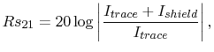 |
(8.13) |
where Itrace denotes the current on the critical trace and Ishield denotes the
current on the shield. According to the same flow direction definition of both currents
Itrace and Ishield, there is a positive sign in the nominator
of (8.13). The following
Figures 8.9, 8.10, and 8.11
show radiated emission reductions achieved by the shielding of traces with different
dimensions. A 10mV voltage source with an impedance equal to the characteristic impedance
of the trace Zw drives the trace and the trace is terminated with a 10pF capacitance.
The trace is routed straight from (xs=50mm, ys=20mm) to (xs=50mm, ys=30mm). The trace supply, termination, and routing is kept equal to this definition
for all examples. Figure 8.9 indicates an emitted power reduction of
about 6dB from one shield, parallel to a trace with 0.2mm width, 0,65mm above the ground
plane. A second shield wire on the other side of the trace leads to an emission reduction
of about 13dB, as depicted in Figure 8.10. However, the current
magnitude difference of the shield current and the critical trace current increases with
increasing trace width and with decreasing trace height above the ground plane. Thus,
Figure 8.11 shows an emitted power reduction of only 2dB from one
shield, parallel to a trace with 2mm width, 0,65mm above the ground plane.
![\includegraphics[height=6.4 cm,viewport=180 285 415
500,clip]{pics/Shield/Narrow_one_shield_VI.eps}](img632.png)
![\includegraphics[height=6.4 cm,viewport=180 285 415
500,clip]{pics/Shield/Narrow_one_shield_VI.eps}](img633.png)
| (a) Radiated power. | (b) Estimated reduction from 8.13. |
Figure 8.9:
Comparison of the radiated emission without and with one 0.2mm shield trace
(width=0.2mm, height above the ground plane=0.65mm) parallel to the trace with a distance
of 0.2mm and terminated to ground.
![\includegraphics[height=6.4 cm,viewport=180 285 415
500,clip]{pics/Shield/Narrow_one_shield_VI.eps}](img634.png)
![\includegraphics[height=6.4 cm,viewport=180 285 415
500,clip]{pics/Shield/Narrow_one_shield_VI.eps}](img635.png)
| (a) Radiated power. | (b) Estimated reduction from 8.13. |
Figure 8.10:
Comparison of the radiated emission without and with 0.2mm shields parallel on
both sides of the trace (width=0.2mm, height above the ground plane=0.65mm) at a distance
of 0.2mm and terminated to ground.
![\includegraphics[height=6.4 cm,viewport=180 285 415
500,clip]{pics/Shield/Narrow_one_shield_VI.eps}](img636.png)
![\includegraphics[height=6.4 cm,viewport=180 285 415
500,clip]{pics/Shield/Narrow_one_shield_VI.eps}](img637.png)
| (a) Radiated power. | (b) Estimated reduction from 8.13. |
Figure 8.11:
Comparison of the radiated emission without and with one 0.2mm shield trace
parallel to the trace (width=2mm, height above the ground plane=0.65mm) with a distance
of 0.2mm and terminated to ground.
Therefore, coplanar shielding provides only reasonable common mode emission reduction for
traces, of which the length-capacitance to ground is strongly influenced by the shield
traces. This is only the case for traces with low trace width and large distance from the
ground plane. Routing of a trace between two ground planes provides an opportunity for
emission reduction, as well as of wide traces. However, each interconnect between two
components must have vertical sections which leave the PCB to enable the connection of
these components. These vertical interconnects cause common mode coupling which is not
reduced by the shield on the PCB. Therefore, interconnects routed between two ground
layers and coplanar shielded on the PCB cannot completely eliminate the common mode
coupling.
C. Poschalko: The Simulation of Emission from Printed Circuit Boards under a Metallic Cover