|
|
|
|
Dissertation Christian Poschalko | Previous: 8.6 Rule 6: Shielding reduces the common mode Up: 8 Design rules for PCBs inside a metallic Next: 8.8 Summary of the design guidelines |
|
|
|
|
Dissertation Christian Poschalko | Previous: 8.6 Rule 6: Shielding reduces the common mode Up: 8 Design rules for PCBs inside a metallic Next: 8.8 Summary of the design guidelines |
![\includegraphics[height=9cm,viewport=125 490 500
740,clip]{{pics/Lead_Frame_rule.eps}}](img638.png) |
The coupling to the enclosure field is reduced by
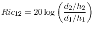 |
(8.14) |
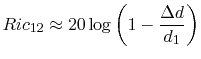 |
(8.15) |
Table 8.1 contains some examples for the achieved common mode coupling reduction with a ground plane directly under the IC. High reduction can be obtained for IC packages with low seating heights and for PCBs with only one inner layer ground plane which has a significant distance from the component layers.
C. Poschalko: The Simulation of Emission from Printed Circuit Boards under a Metallic Cover