In Section 5.2.1 it was shown that by increasing the gate-source spacer length
the parasitic capacitance between these two contacts is reduced, and so does the
on-current. In Section 5.2.2 it was shown that by increasing the gate-drain
spacer length the
 ratio increases. At the same time, by increasing
the gate-drain spacer length the parasitic capacitance between these two
contacts decreases, which results in a reduced gate-delay time. Fig. 5.14 shows
the effect of the gate-drain spacer length on the gate-delay time versus the
ratio, which indicates a significant performance
improvement by increasing the gate-drain spacer length.
ratio increases. At the same time, by increasing
the gate-drain spacer length the parasitic capacitance between these two
contacts decreases, which results in a reduced gate-delay time. Fig. 5.14 shows
the effect of the gate-drain spacer length on the gate-delay time versus the
ratio, which indicates a significant performance
improvement by increasing the gate-drain spacer length.
Since the gate-delay time is proportional to the parasitic capacitance and
inversely proportional to the on-current (5.1), there is an optimal value
for the gate-source spacer length,
 , which minimizes the
gate-delay time. The optimal value for the gate-source spacer length is achieved if
, which minimizes the
gate-delay time. The optimal value for the gate-source spacer length is achieved if
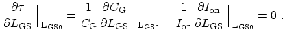 |
(5.6) |
Fig. 5.15 shows the sensitivity of the on-current with respect to the gate-source spacer
length for devices with zero and positive barrier heights for
electrons. For thinner insulators the width of the source-sided barrier decreases, resulting
in a higher tunneling current contribution to the total current and a higher
sensitivity of the on-current to
 (see Section 5.2.1).
The optimal gate-source spacer length for a device with zero barrier height for
electrons is
 for
for
 and
and
 . For devices
with positive barrier heights the optimal value of the gate-source spacer
length is smaller than that of a device with zero barrier height due to the
higher sensitivity of the on-current with respect to the gate-source spacer
length.
. For devices
with positive barrier heights the optimal value of the gate-source spacer
length is smaller than that of a device with zero barrier height due to the
higher sensitivity of the on-current with respect to the gate-source spacer
length.
Note that the optimal value for
depends on
 . For small values of
the gate-drain parasitic
capacitance dominates the gate-source parasitic capacitance. Therefore, any
further decrease of the gate-source spacer length does not improve the gate-delay
time. As shown in Fig. 5.16, the optimal value of the gate-source spacer
length for the given material and geometrical parameters results in optimized
device characteristics.
. For small values of
the gate-drain parasitic
capacitance dominates the gate-source parasitic capacitance. Therefore, any
further decrease of the gate-source spacer length does not improve the gate-delay
time. As shown in Fig. 5.16, the optimal value of the gate-source spacer
length for the given material and geometrical parameters results in optimized
device characteristics.
M. Pourfath: Numerical Study of Quantum Transport in Carbon Nanotube-Based Transistors
![\includegraphics[width=0.5\textwidth]{figures/tau-Z-LD.eps}](img997.png)
![\includegraphics[width=\textwidth]{figures/tau-ZP-Ls.eps}](img998.png)
![\includegraphics[width=0.5\textwidth]{figures/tau-Z-LS.eps}](img999.png)